The technical specifications of the filter include margin, cutoff frequency, in-band fluctuation, in-band standing wave ratio, in-band phase linearity, Butterworth, Chebyshev, Bessel filter circuit analysis, transfer function. Includes low pass, high pass, and band pass.
Technical indicator supplement
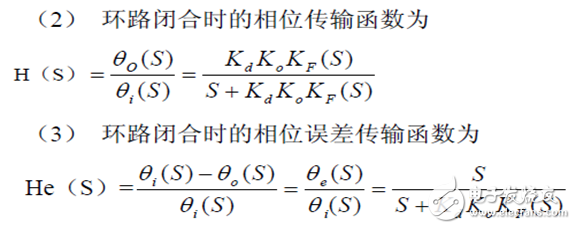
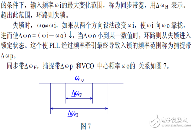
Margin: Phase margin is phase-locked loop ![]() The open-loop transfer function is in the Bode diagram (consisting of two graphs: one is the logarithmic amplitude-frequency characteristic, its ordinate is 20lg|G(jw)|, the unit is decibel, expressed in symbol dB. The other is The logarithmic phase-frequency characteristic, the ordinate is the angle.) The performance parameters formed on the PLL are used to evaluate the phase-locked loop.
The open-loop transfer function is in the Bode diagram (consisting of two graphs: one is the logarithmic amplitude-frequency characteristic, its ordinate is 20lg|G(jw)|, the unit is decibel, expressed in symbol dB. The other is The logarithmic phase-frequency characteristic, the ordinate is the angle.) The performance parameters formed on the PLL are used to evaluate the phase-locked loop. ![]() The basis for stability. Its definition and calculation method is: draw the phase-locked loop separately
The basis for stability. Its definition and calculation method is: draw the phase-locked loop separately ![]() The amplitude-frequency and phase-frequency curves of the open-loop transfer function find the frequency point at which the amplitude gain is 0 db. The phase value corresponding to the frequency point minus the difference of -180° is the phase margin. If the difference is greater than 0, the loop is stable, and if it is less than 0, the loop is unstable.
The amplitude-frequency and phase-frequency curves of the open-loop transfer function find the frequency point at which the amplitude gain is 0 db. The phase value corresponding to the frequency point minus the difference of -180° is the phase margin. If the difference is greater than 0, the loop is stable, and if it is less than 0, the loop is unstable.
The phase-locked loop ![]() , I found some phase-locked loops below.
, I found some phase-locked loops below. ![]() data of.
data of.
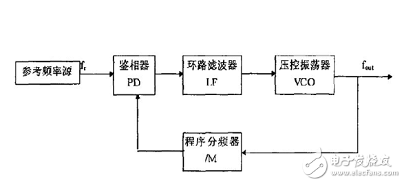
PLL block diagram
Phase-locked loop ![]() (phase-locked loop) is a method for making the frequency more stable in radio transmission. There are mainly VCO (Voltage Controlled Oscillator) and PLL IC. The voltage controlled oscillator gives a signal, one part is output and the other part is divided. Compared with the local oscillator signal generated by the PLL IC, in order to keep the frequency constant, the phase difference is not changed. If there is a phase difference, the voltage at the voltage output of the PLL IC changes to control the VCO until Phase difference recovery! Reach the purpose of frequency lock! ! A closed loop electronic circuit that maintains a determined relationship between the frequency and phase of the controlled oscillator and the input signal.
(phase-locked loop) is a method for making the frequency more stable in radio transmission. There are mainly VCO (Voltage Controlled Oscillator) and PLL IC. The voltage controlled oscillator gives a signal, one part is output and the other part is divided. Compared with the local oscillator signal generated by the PLL IC, in order to keep the frequency constant, the phase difference is not changed. If there is a phase difference, the voltage at the voltage output of the PLL IC changes to control the VCO until Phase difference recovery! Reach the purpose of frequency lock! ! A closed loop electronic circuit that maintains a determined relationship between the frequency and phase of the controlled oscillator and the input signal.
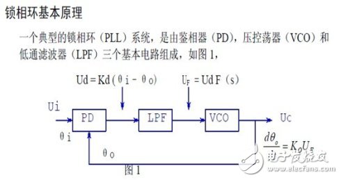
Phase-locked loop ![]() It consists of a phase detector, a loop filter and a voltage controlled oscillator. The phase detector is used to discriminate the phase difference between the input signal Ui and the output signal Uo and output the error voltage Ud. The noise and interference components in the Ud are filtered by a low-pass loop filter to form the control voltage Uc of the voltage controlled oscillator (VCO). The result of Uc acting on the voltage controlled oscillator is that its output oscillation frequency fo is pulled toward the loop input signal frequency fi. When the two are equal, the loop is locked, which is called the lock. The DC control voltage that maintains the lock is provided by the phase detector, so there is a certain phase difference between the two input signals of the phase detector.
It consists of a phase detector, a loop filter and a voltage controlled oscillator. The phase detector is used to discriminate the phase difference between the input signal Ui and the output signal Uo and output the error voltage Ud. The noise and interference components in the Ud are filtered by a low-pass loop filter to form the control voltage Uc of the voltage controlled oscillator (VCO). The result of Uc acting on the voltage controlled oscillator is that its output oscillation frequency fo is pulled toward the loop input signal frequency fi. When the two are equal, the loop is locked, which is called the lock. The DC control voltage that maintains the lock is provided by the phase detector, so there is a certain phase difference between the two input signals of the phase detector.
The voltage controlled oscillator gives a signal, one part is used as the output, and the other part is compared with the local oscillator signal generated by the PLL IC by frequency division. In order to keep the frequency constant, the phase difference is not changed, if there is a phase difference Change, the voltage at the voltage output of the PLL IC changes, to control the VCO until the phase difference is restored! Reach the purpose of frequency lock! ! A closed loop electronic circuit that maintains a determined relationship between the frequency and phase of the controlled oscillator and the input signal.
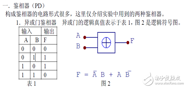
2. The edge-triggered phase detector has been mentioned before. The XOR gate phase comparator requires two signals to be compared to have a 50% duty cycle, which brings some inconvenience to the application. The edge-triggered phase detector compares the signal by comparing the upper edge (or lower edge) of the two input signals, and does not require the duty cycle of the input signal.
Debortu
Cutoff frequency: The passband edge frequency at which the relative attenuation reaches a certain value. In the frequency response of the filter, the amplitude at this frequency is 3 dB lower than the amplitude of the center frequency in the passband region, so it is also called the 3 dB frequency.
In-band fluctuation: The maximum value of the difference between the peaks and troughs in the passband is defined as in-band fluctuation. Its value is expressed in decibels. Generally, in a digitally modulated communication system, the ripple value of the filter used is preferably not higher than 0.5 dB. Filters with ripples in the passband are dominated by Chebyshev characteristics.
In-band standing wave ratio (VSWR): An important measure of whether a signal in the passband of a filter is well matched. Ideal match VSWR = 1:1, VSWR "1" when mismatched. For an actual filter, the VSWR "1.5:1 bandwidth is generally less than BW3dB, and its ratio to BW3dB is related to the filter order and insertion loss. The voltage standing wave ratio (VSWR) of a filter is an indicator of how well the filter matches the characteristic impedance of the system it is in. The VSWR of a port of a filter is the impedance seen from that port when another port accurately matches the system characteristic impedance (typically 50 Ω in high frequency systems). Therefore, the indicator of a filter usually includes both the typical value and the maximum value of the input VSWR and the output VSWR, which respectively represent the degree to which the filter matches the source and load impedance to which it is connected. VSWR is expressed as a ratio of 1 to 1, such as 1.50:1, but can also be expressed as the reflection loss (in dB) of the filter. If a filter exhibits impedance matching on both the passband and the stopband, then this filter is considered an absorption filter. This filter is considered to be a reflective filter when impedance matching is only performed on the passband. Device. The latter filter has a higher VSWR on the stop band, such as 20.0:1 or higher. The power handling capability of the filter is typically related to the physical size of the filter, the operating frequency range, the filter technology, the type of substrate material, the type of package, and the thermal limits of the material. The maximum power limit is also a function of the type of signal (such as continuous wave (CW) or pulsed signal) and the type of modulation used by the signal.
In-band phase linearity: This indicator characterizes the phase distortion introduced by the filter for the transmitted signal in the passband. Filters designed with linear phase response functions have good phase linearity, but have poor frequency selectivity and are limited to pulsed, or phase-modulated signal transmission system applications. The characteristic of linear phase: a single frequency sinusoidal signal passes through a system, assuming that its time through the system requires t, then the output phase of this signal is behind the phase of the original signal wt. It can be seen from this that the phase of a sinusoidal signal passing through a system is equal to its w*t; conversely, if a sinusoidal signal of frequency w passes through the system and its phase falls behind delta, the signal is delayed. The time of delta/w. In an actual system, an input signal can be decomposed into a superposition of multiple sinusoidal signals. In order for the output signal to not produce phase distortion, it must be required that the sinusoidal signals it contains pass through the system for the same time. Therefore, the phase of each sinusoidal signal lags behind, w1*t, w2*t, w3*t. Therefore, the backward phase is proportional to the frequency w, and if advanced, the magnitude of the leading phase is also proportional to the frequency w. From the perspective of the frequency response of the system, it is required that its phase-frequency characteristic is a straight line. In the design of the FIR filter, in order to obtain the linear phase property, the phase-frequency characteristic of the real-coupled symmetric sequence is usually characterized by a constant 0 and a real odd-symmetric sequence, and the phase-frequency characteristic is constant at 90 degrees. Therefore, a symmetric sequence is obtained, which is not a causal sequence. It is an unrealizable system. In order to be called a physically achievable system, it needs to be moved to the right for half a cycle, which causes the phase shift characteristic to change with time and also linearly. .
Insertion loss:
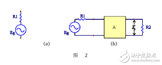
Figure 2 (a) shows a power supply with an electromotive force of Eg and an internal resistance of R1. Set the load to R2, then when the load is directly connected to the power supply, the power it can absorb is:
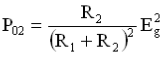
Now we connect filter A between the power supply and the load. As shown in Figure 2(b), due to the characteristics of the filter, when the power frequency changes, the voltage drop E2 appearing across R2 is different, that is, R2 is Power obtained by the power supply
![]()
It is not equal in different frequencies. The ratio of P02 to P2 expressed in decibels is called the insertion loss Li:
The insertion loss Li is a parameter that measures the performance of the filter. From the above discussion, it is apparent that the insertion loss of a good filter should be relatively low in the passband and should be high in the stopband. The insertion loss of an ideal filter should be equal to zero in the passband and infinite in the stopband. Insertion loss is a commonly used parameter for ordinary filters. The impedance transformation characteristics of the filter network are not difficult to match the load R2 to the power supply throughout the passband. At this time, the power absorbed by the load will exceed P02, and Li will take a negative value. According to the ratio of R1 and R2, this negative value of Li is also different. Therefore, the insertion loss Li is not a convenient comparison benchmark. In order to avoid this difficulty, another parameter is proposed, which is based on the maximum power P0 that the power supply can supply.
Butterworth filter
1. Butterworth low-pass filter (referred to as BW filter)
(1) Basic properties
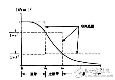
Figure 5.32 Amplitude squared frequency response of the low pass filter
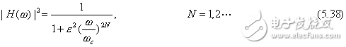
The so-called Butterworth filter is a system function of the Butterworth approximation function, which approximates the ideal rectangular characteristic in the form of the highest order of the series. Equation (5.38) is its general modular function representation.
It can be seen that its numerator is equal to the constant, and the denominator is
![]()
(or
![]()
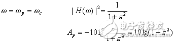
The polynomial is a positive real function, and the system functions derived from it are physically achievable. Where N denotes that the order of the filter is a positive integer, ωc is the cutoff frequency or the attenuation
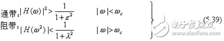
The bandwidth is equal to 3dB, ε is the parameter related to the passband attenuation Ap, and λ is the parameter related to the stopband attenuation Ar, as shown in Figure 5.32. In the figure, ωc is the cutoff frequency and also the boundary frequency of the passband, and ωc is the boundary frequency of the stopband, so there is
When ε→0, λ→∞, ωr→ωc, the filter characteristics approach the ideal rectangle.
Obviously, the parameters ε and λ mainly depend on the tolerance range of the design index. If the indicator is specified at the passband boundary frequency, the maximum attenuation allowed by the passband is Ap, according to equation (5.39).
Therefore
![]()
For a BW type filter, the bandwidth of Ap=3db is usually taken as the cutoff frequency, so ε=1. If the stopband boundary frequency is specified, the minimum attenuation allowed by the stopband is Ar, then according to equation (5.39)
![]()
Therefore
![]()
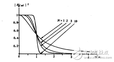
Figure 5.33 Normalized amplitude characteristic curve of Butterworth low-pass filter
The analog filter design process, for versatility, is often expressed in a normalized form. For BW type
![]()
In order to normalize the frequency, the formula (5.38) is rewritten into
![]()
In the middle
![]()
The normalized modular function is shown in Figure 5.33. As the amplitude increases with N, the passband becomes more flat and closer to the ideal characteristic. When N→∞, the rectangle is approximated.
![]()
The basic properties of the BW type low pass filter will be described below in combination with equation (5.43).
(a) exists for different values ​​of N
![]()
This shows that the amplitude characteristic monotonically decreases with increasing frequency ω in the positive frequency range (including passband and stopband). ω = 0 (DC) is the largest, ω = ∞ tends to zero, that is, there is no finite zero.
(b) When ω = 0, that is, for DC, the difference between the ideal amplitude characteristic and the resulting approximate characteristic is equal to zero for the Bavos function itself, or for the 2N-1 derivative. Because formula (5.43) can be obtained according to the binomial theorem or the scale of the class
![]()
and so
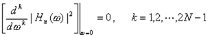
This shows that the most "flat" near ω = 0 and ω = ,, so the Butterworth filter is also called the "maximum flat" approximation.
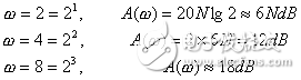
(c) When the frequency is far from ω, that is, the high frequency range of ω》》1, the frequency is increased by 6NdB for every doubling (octave) frequency. Or, the "roll-off rate" is 6NdB/octave because at this time
![]()
and so
![]()
when
Chebyshev:
Figure 6.2.5 shows the amplitude-frequency characteristics of the Chebyshev I-type filter when the order N is odd and even. The square function of the amplitude is expressed by A2 (Ω):
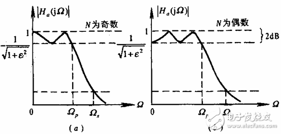
Figure 6.2.5 Chebyshev I-mode filter amplitude-frequency characteristics
Bessel filter:
Due to their linear phase response characteristics, such filters have optimal impulse response (minimize overshoot and ringing) performance. For a given number of poles, Bessel's amplitude-frequency response is not as flat as Butterworth, and the attenuation of the band outside the -3 dB cutoff frequency is not as steep as Butterworth. Although a higher-order Bezier filter is required to approximate the amplitude-frequency response of a given Butterworth filter, given the impulse response fidelity of the Bezier filter, a certain complexity is added (due to Additional filter components) are also worthwhile.
Comparison of the three responses:
Butterworth responded:
Advantages: The Butterworth filter provides maximum passband amplitude response flatness, good overall performance, better impulse response than Chebyshev, and better attenuation than Bessel.
Disadvantages: There is a certain overshoot and oscillation in the step response.
Chebyshev responds:
Advantage: Compared to Butterworth, Chebyshev filters have better pass-band attenuation.
Disadvantages: The ripple in the passband is unsatisfactory, and the ringing of the step response is more serious.
Bessel response:
Advantages: The Bezier filter has an optimal step response – very small overshoot and ringing. Disadvantages: Compared with Butterworth, the Bessel filter has a slower attenuation outside the passband
Innosilicon Machine:Innosilicon A10 ETHMaster (500Mh),Innosilicon A10 Pro ETH (500Mh),Innosilicon A10 Pro+ ETH (750Mh),Innosilicon A11 Pro ETH (1500Mh)
Innosilicon is a worldwide one-stop provider of high-speed mixed signal IPs and ASIC customization with leading market shares in Asian-Pacific market for 10 consecutive years. Its IP has enabled billions of SoC's to enter mass production, covering nodes from 180nm to 5nm across the world`s foundries including: GlobalFoundries, TSMC, Samsung, SMIC, UMC and others. Backed by its 14 years of technical expertise in developing cutting-edge IPs and ASIC products, Innosilicon has assisted our valued partners including AMD, Microchip and Microsoft to name but a few, in realizing their product goals.
Innosilicon team is fully devoted to providing the world's most advanced IP and ASIC technologies, and has achieved stellar results. In 2018, Innosilicon was the first in the world to reach mass production of the performance-leading GDDR6 interface in our cryptographic GPU product. In 2019, Innosilicon announced the availability of the HDMI v2.1 IP supporting 4K/8K displays as well as our 32Gbps SerDes PHY. In 2020, we launched the INNOLINK Chiplet which allows massive amounts of low-latency data to pass seamlessly between smaller chips as if they were all on the same bus. With a wide range of performance leading IP in multiple FinFET processes and 22nm planar processes all entering mass production, Innosilicon's remarkable innovation capabilities have been proven in fields such as: high-performance computing, high-bandwidth memory, encrypted computing, AI cloud computing, and low-power IoT.
Innosilicon Machine,A11 Pro 1500M Miner,Asic Miner A11 Pro 8G,A11 Pro 8G 1500Mh,ETC miner
Shenzhen YLHM Technology Co., Ltd. , https://www.hkcryptominer.com