Medical technology has always been one of the important application fields of CCD (Charge Coupled Device) image sensors. Now, CMOS sensors have entered a period of rapid development. The reason is that, first of all, the CMOS image quality is comparable to the CCS image. Second, using standard semiconductor manufacturing processes, CMOS sensors have a great advantage in terms of price. Third, the unlimited potential of CMOS sensors in circuit integration can reduce the number of input and output interfaces. Based on a special CMOS image sensor that can be discarded after one use, a new type of low-cost colonoscope has been developed. This type of colonoscopy does not require costly sterilization of colon disease diagnosis and treatment equipment, thus avoiding any possibility of infection. This device is small in size and can perform almost painless inspections.
Because CCD image sensors have many advantages such as high resolution, low noise, low dark current, and large photosensitive range, medical image acquisition has always been an important application field of such image sensors. On the other hand, the development of CMOS sensors in recent years, especially the achievements in using small-sized pixels to achieve high resolution and reducing noise and dark current levels, has made CMOS sensors a more widely used low Cost equipment. From the various fields of X-ray image acquisition and endoscopy to the "camera in pills" with its own characteristics, the application field of CMOS sensors can be described as all-encompassing.
Features of CMOS technology
The natural advantage of complementary metal oxide semiconductor (CMOS) technology is that this technology can add CMOS logic circuits to the sensor chip, thereby integrating image acquisition and control, conversion and sensing functions [1]. Its high integration density makes the realization of small single-chip systems possible. Integrating more system functions to develop an independent photoelectric sensor system, the realization of this goal is currently only constrained by economic factors such as return on investment, market capacity, and development costs.
The single-chip solution stands out from other solutions due to its advantages such as a small number of external components and interconnections. These advantages are very important for small-diameter endoscopes.
High integration is synonymous with low cost, so CMOS image sensors are favored by various types of endoscope applications. Due to the low power consumption, CMOS image sensors are also suitable for the manufacture of autonomous small cameras, which can be installed in pill-sized boxes and can wirelessly transmit data to receiving stations.
In addition, CMOS technology can also be used in the production of anti-radiation products, which generally have stronger ionizing radiation resistance (ionizingradiaTIon) than CMOS image sensors [2]. The use of thicker epitaxial layers or backlighting to improve the CMOS technology slightly can improve the near-infrared (NIR) sensitivity of the sensor, resulting in new medical image processing applications (such as near-infrared-based tomography [3] ). Cost-effective splicing technology can use 8-inch wafers and 12-inch wafers in the future to produce large (up to wafer-level) CMOS image sensors.
Small image sensor for endoscope
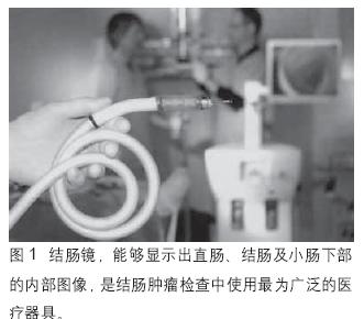
In order to manufacture a new type of disposable endoscope (Figure 1), STMMedizintechnik of Kissing, Germany [4] requires a low-cost image sensor, which can only be produced using CMOS technology. To this end, Cypress / FillFactory, an expert in the field of CMOS image sensors, has successfully developed a small color image sensor BOCA using 0.35 μm CMOS processing technology. BOCA has a sensor area of ​​9mm2 and consists of 512 × 512 square pixels with a length of 6μm on each side. The filling factor of up to 58% of this sensor is a strong guarantee for the high sensitivity of the product (Figure 2).
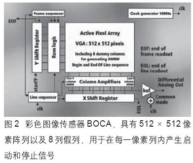
The sensor spectral response range is 400 to 1000 nm. The pixel frequency is 10MHz and the output is 20fps at 50ms integration time. The shutter selection triggers the rolling shutter (triggered rolling shutter). At a full speed of 20fps, the power consumption of this image sensor is about 36mW. Clock generator and fixed pattern noise (FPN) correction are integrated on the chip. The image sensor prototype is used to ensure that the product meets the target specifications, from which it can be seen that the negligible deviations generated during the manufacturing process. The noise measurement result is 63eˉ, which is within the acceptable range; the signal-to-noise ratio is 522: 1, and the dynamic range is 54dB. The dark current at room temperature is 78pA / cm2; the dark current at body temperature (37 ° C) is 188pA / cm2.
Fill factor and quantum efficiency
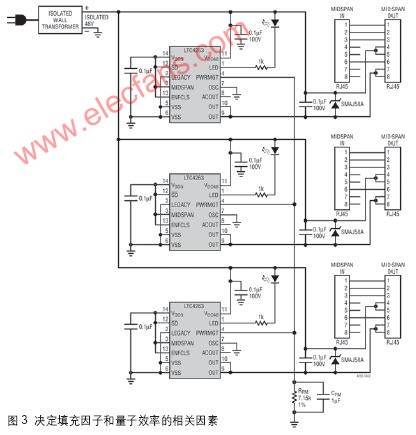
In order to obtain higher sensitivity, shorter exposure time, and the smallest possible pixel size, the image sensor should make full use of available photons. The product of the fill factor and the quantum effect, FF × QE (Figure 3), is an important factor in measuring pixel sensitivity and an important factor in measuring pixel sensitivity. Quantum efficiency refers to the normalized value of the actual and theoretical maximum number of electrons generated when a pixel is struck by a photon. QE is less than a single integer, depending on the wavelength and the given material. Many photons are lost in practical applications due to the following reasons:
* Failed to be absorbed into the photosensitive layer, and the charge carrier was lost during the reorganization process
The geometric fill factor FF is the ratio of the effective (photosensitive) pixel area to the total pixel area (pixel boundary and circuit).
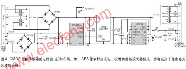
CMOS image sensors belong to active pixels (active pixel sensor, APS) (Figure 4), that is, photodiodes and subsequent amplifiers, whose noise level and sensitivity are comparable to CCD converters. The disadvantage of this sensor is that the amplifier transistor occupies too much pixel area, and the photodiode has very little space to use. Active pixel fill factor is also restricted by the following factors:
* Photon reflection or absorption caused by metal plating or silicide;
* The photoelectrons accumulated in the amplifier barrier cannot play a role in signal generation;
* Small available photosensitive barrier;
* Photoelectrons (or holes) recombine with available charge loads, limiting the diffusion length.
Fill factor optimization
Increasing the number of fill factors is the most urgent development goal of today's CMOS image sensors. There are currently several ways to improve the fill factor, and the use of large photodiodes on active pixels is one of them. This method can produce a better fill factor, but due to the higher photodiode volume (large pixels), the sensitivity of charge conversion is lower. We can use passive pixels or CCD frame transmission architecture to solve this problem, but this approach will reduce the signal-to-noise ratio or increase costs.
Another method is to use micro lenses to condense the light into a small photodiode. In the case of normal incidence, the fill factor can be as high as 90%, but this method also has several shortcomings, such as non-standard manufacturing processes, the above-mentioned vertical incidence, and the low effectiveness of the lens for large aperture targets (thus The microlens must have a reasonable and appropriate design).
FillFactory [5] has a patented technology that can provide a higher fill factor for CMOS-APS. In contrast to traditional APS pixels where the photosensitive area is limited to the diode area (Figure 5a), FillFactory's method can convert most of the area of ​​a standard CMOS-processed chip into a photosensitive area (Figure 5b).
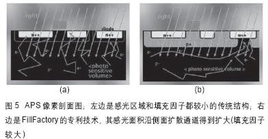
The relatively small photodiode can process the light from any angle, and only produces a very small dark current. This kind of diode can also detect the photoelectrons generated in the epitaxial layer under the full pixel, and the traditional devices generally "ignore" this photoelectron. This feature greatly increases the number of fill factors. The photoelectrons are separated by the electrostatic barrier and the bottom plate from the upper active pixel circuit, and are introduced into the photodiode barrier along the potential well on the side. In practical applications, almost all electrons diffuse into this area. Due to the short diffusion time (usually 10 to 50 nanoseconds), there are basically no side effects such as image smearing. This pixel architecture can bring three advantages:
* 100% fill factor rate-except for light absorbed by the non-participating barrier of the amplifier, light reflected by the metal compound, and light lost during the recombination of free electrons;
* Compared with large diode pixels, the dark current is smaller;
* The conversion sensitivity (charge to voltage) within the barrier is high, and the signal to noise is relatively high.
Application: disposable colonoscope
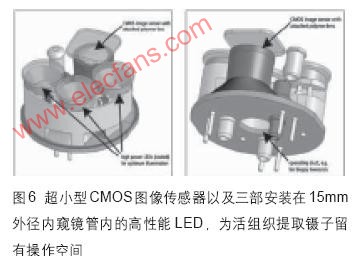
The goal of the development of disposable colonoscopy invendoSC20 is to make the colonoscopy process more gentle and without medication, and at the same time solve the difficult hygiene problems through one-time use. In the design of disposable systems, the low-cost CMOS image sensor should be small enough to be installed inside the endoscope, which is very important. The operation of the new colonoscope can be easily accomplished using a joystick. This colonoscope can slide very gently along the colon in the flexible endoscope tube (operating length 1600mm, outer diameter 15mm) without the endoscope operating along the colon wall Relative movement.
The low-cost, high-resolution CMOS image sensor BOCA can provide a 100x digital zoom together with a plastic lens, while achieving a 120 ° field of view. Longer colonic segments can be illuminated with high-performance light-emitting diodes (LEDs) (Figure 6). These parts are installed on the top of the nail-sized colonoscope. The colonoscope also integrates an operation tube for the extraction forceps of the living tissue for tissue sample extraction.
Two to three million colonoscopy examinations are performed annually in Germany alone; according to experts in the field of medical publishing and national statistics, approximately 25 million such examinations or surgeries are performed worldwide each year. The further application of low-cost, very small CMOS image sensors in the field of gastroscopes or endoscopes will also become a reality, thus opening up a brand-new market comparable to the market of household electronic products.
prospect
CMOS image sensors are rapidly moving forward and gradually entering large markets. Taking advantage of the advantages of high resolution, high frame rate, high sensitivity and low cost, as well as the ability to provide customers with customized specifications of product design, CMOS image sensors can provide customers with multi-functional standard solutions suitable for a variety of applications. And use this as a driving force to quickly move forward.
Cummins 401-999KW Diesel Generator
Cummins 401-999Kw Diesel Generator,Cummins Shanghai Genset,Cummins Shanghai Power Generator,999Kw Diesel Generator
Shanghai Kosta Electric Co., Ltd. , https://www.ksdgenerator.com