1 Introduction
This article refers to the address: http://
Charge Coupled Device is a semiconductor device invented by WS Boyle and GESmith of Bell Labs in the United States in 1970 [1]. It is regarded as the most important semiconductor device that has appeared since the 1970s [2]. CCD has the advantages of low signal output noise, large dynamic range, high quantum efficiency and high charge transfer efficiency. Therefore, CCD-based cameras are used in machine vision systems, security systems, intelligent transportation systems, and Internet access devices. Widely used. With the rapid development of CCD technology, CCD cameras are also developing in the direction of higher speed, more convenient control and better quality performance.
While some CCDs only require timing signals and do not require power drive, most high performance CCDs require power drive and the drive waveform requirements are bipolar and large. Therefore, the TTL signal generated by the CCD timing generating unit [3] needs to be level shifted and amplified. The CCD is a capacitive load, so a large transient current is generated under the action of a high-speed driving pulse, which requires the driving circuit to have a sufficiently strong current driving capability. At present, CCD driver driving to realize CCD power driving can meet some camera requirements. However, when the CCD drive waveform is bipolar, the driver integrated circuit operating with a single power supply still requires an external level shift circuit. When the driving waveform voltage amplitude of the CCD exceeds the working voltage of the CCD driving integrated circuit, these driving integrated circuits cannot meet the requirements. Therefore, based on the analysis of the CCD power driving circuit and its requirements, this paper designs a discrete component. More general CCD camera power drive circuit.
2 CCD power drive circuit and its requirements
Figure 1 shows a block diagram of a typical CCD camera. The CCD camera generally consists of a CCD sensor chip, a CCD timing generator, a CCD power driver, an analog processing front end, a digital image processing unit, a controller, a power supply portion, and an external optical imaging system. It can be seen from the figure that the function of the CCD power driving part is to power-amplify various transfer pulse signals output by the CCD timing generating unit to meet the requirements of the CCD for driving waveform voltage and current and timing. The quality of the driving signal will have a greater impact on the charge transfer efficiency of the CCD, thus affecting the quality of the imaging.
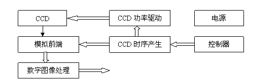
Figure 1 CCD camera block diagram
Fig.1 the block diagram of the CCD camera
The requirement for the power drive circuit is that the waveform voltage swing satisfies the requirements of the CCD, and the rising and falling edges of the waveform are fast enough to meet the requirements of the CCD. Since the CCD is a capacitive load, the transient current that the driver needs to provide can be calculated from the formula of the capacitor model below.

In the above calculation, the time of the rising or falling edge is defined as 10% to 90% of the level of the level, and the edge change is linear. The load is 300pF, the voltage amplitude is 20V, and the rising or falling edge is 20ns. The current generated at the edge change is 0.24 amps. The current will be larger at higher speeds.
In summary, the requirement for the CCD power drive circuit is to provide a sufficiently large transient drive current at a fast change edge with a large voltage swing. Therefore, the temperature of the CCD power driver tends to be higher [4], and the device with sufficient operating current should be selected to meet the requirements when selecting the device.
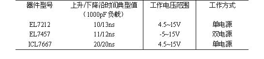
Table 1 lists several CCD power driver integrated circuits that are currently in widespread use. From the table we can see that the rise and fall edges of the EL7457 change the fastest, and it works for dual supplies, so no additional level shifting circuitry is required, but the EL7457 has the disadvantage of a narrow operating voltage range. Note that the voltage listed in the table -5~15V is the maximum range of positive and negative power supplies. In fact, the difference between the positive and negative power supplies is 15V [5], so if the negative power supply is -5V, the positive power supply can only When it reaches 10V, the positive power supply can reach 15V only when the negative power supply is 0V. And the negative power supply of EL7457 can only reach -5V. The rise and fall times of the EL7212 are similar to those of the EL7457, but they operate from a single supply. In the case of bipolar drive waveforms, additional level shifting circuitry is required. The ICL7667 also operates from a single supply with slower rising and falling edges and can only be used in relatively slow CCD cameras.
Table 1 Several CCD power drive integrated circuit performance indicators
Tab.1 Performance of some CCD driver IC
3 CCD power drive circuit analysis and design
According to the above specific requirements for the CCD power drive circuit, we have designed the following circuit form through careful analysis. The timing signal of the timing generation unit in the figure is simulated by a pulse wave generator and an equivalent internal resistance R2, and the load capacitance is set to 300 pF here.
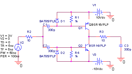
Figure 2 CCD camera power drive circuit diagram
Fig.2 the circuit of CCD camera power driving
First, the timing signal of the timing generation unit is coupled to the diode clamp via capacitors C1 and C2. Two diodes D1 and D2 and two resistors R1 and R4 are used to clamp the capacitively coupled signal to a fixed level. Here the positive level is +10V and the negative level is -10V. The diode D1 clamps the signal to a positive level, causing the signal to swing downward on a positive level. The same diode D2 clamps the signal to a negative level, causing the signal to swing upward at a negative level. Note that the direction of the diode is correct. The two signals thus generated are used to control the conduction and deactivation of the two switching transistors. The collectors of the two complementary transistors are connected together as a switch output. Note that if the emitters are connected together, they operate as emitter followers instead of switches. When the control signal applied to the base of Q2 swings upward, the transistor Q2 is turned on, and at this time, the signal applied to the base of Q1 is in the high level period, and thus the transistor Q1 is turned off, so the signal output to the load C3 is output. Is low. Similarly, when the control signal applied to the base of Q2 is low, the transistor Q2 is turned off, and at this time, the signal applied to the base of Q1 swings at a high level, so that the transistor Q1 is turned on, so the output is output to the load. The signal of C3 is high. Therefore, the circuit is an inverting drive circuit. Resistor R3 controls the edge change time of the waveform applied to the load capacitor.
In this circuit, the diode uses Philips high-speed Schottky diode, model BAT85/PLP [6]. The parameters are: reverse continuous voltage VR is 30V, and the forward conduction voltage drop VF is 320mV when the forward current IF is 1mA. The reverse recovery time trr is 4 ns. The transistor is also selected from Philips' switch triodes, model numbers BSR14/PLP[7] and BSR16/PLP[8]. The VCEO parameter BSR14/PLP is 40V, and the BSR16/PLP is 60V. The collector current IC parameter BSR14/PLP is 800 mA, and the BSR16/PLP is 600 mA. These parameters can meet the requirements of wide driving voltage range and large transient current.
The various component parameters of the above circuit are given according to the pixel transfer clock of 10 MHz. If other transfer clocks or frequencies are changed, the above parameters can be modified, and the circuit structure form does not change.
4 simulation and experimental results
In order to verify the correctness and rationality of the design. The circuit of the above design was simulated under Cadence's OrCAD PSpice AD ​​software. The simulation results also prove the rationality of the design circuit. Figure 3 is a waveform diagram of the simulation results. It can be seen from the figure that the circuit is inverting drive, and the output has a delay of about 10 ns relative to the input. The output waveform meets the requirements in both amplitude and edge change time.
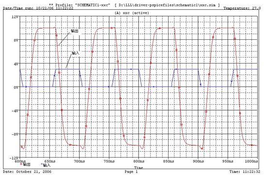
Figure 3 simulation results waveform diagram
Fig.3 the waveform of simulation result
According to the above circuit structure, we use the corresponding components to build the corresponding actual circuit. The experimental results are basically consistent with the simulation results. This shows that this circuit can be used in CCD cameras, which can reduce costs and improve reliability.
5 Conclusion
The innovation of this paper is to realize high-performance CCD power drive circuit with fewer discrete components, which can be used in traditional CCD power drive integrated circuits in some cases.
The CCD power drive circuit has a large impact on the performance of the CCD camera. At present, the CCD power driving integrated chip that can be used sometimes needs an external level shifting circuit, and sometimes cannot meet the requirements of voltage swing and the like, and the implementation cost is high. To this end, this paper designs a CCD power drive circuit realized by discrete components. The circuit has the advantages of low cost, high reliability, wide operating voltage range and the like compared with the circuit currently implemented by the CCD dedicated power driving integrated chip. Therefore, when the existing driver integrated circuit cannot meet the requirements, the circuit can be used to realize the power driving of the CCD camera.
This 60 -port USB charger is charged at the fastest speed to as many as 60 devices. The table charger has 60 ports. The maximum output of a single USB port is 2.4A, and the output power is as high as 300W. Super intelligence: Each port can charging a current of up to 2.4A, and adaptive smart chip detector can provide the best charging current for connected devices. Multiple protection: The USB charger has rush protection, over -current and overvoltage protection functions, which can safely protect your smart devices. Suitable for multiple devices: charging stations are compatible with 99 % of smart devices, such as iPad iPhone, tablet, Bluetooth headset, fan, DVS, for PSP. It is suitable for various occasions, such as hotels, school dormitories, gym and other places.

60 Port Usb Charger,Multi-port USB 600W charger,60 Port Usb Smart Charger,High Power Mobile Phone Charger
shenzhen ns-idae technology co.,ltd , https://www.best-charger.com