The home gateway is the core component of the embedded smart home system, and the designed wireless transceiver module circuit is part of the home gateway. The principle and design method of the wireless transceiver module circuit composed of the single-chip RF transceiver chip nRF0433, the designed wireless transceiver module circuit works in the 433MHz ISM frequency band, the data rate is 9600bit/s, the sensitivity is up to -105dBm, the maximum transmission power is up to 10mW, and the power supply voltage is 215. ~ 515V, working current 31 ~ 47mA.
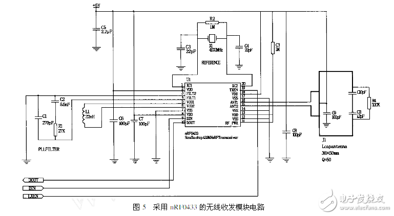
Antenna input/output, when nRF0433 is in receive mode, the ANT1 (pin 16) and ANT2 (pin 15) pins provide RF input to the low noise amplifier LNA; when nRF0433 is in transmit mode, the RF output is provided from the power amplifier To the antenna. The antenna connected to the nRF0433 is a differential form and the recommended load impedance in the antenna channel is 400Ω. The differential loop antenna on the printed circuit board (PCB) is shown in the printed circuit board diagram of the application circuit. The power amplifier output stage consists of two open-collector transistors of the differential structure, and the power supply VDD to the power amplifier must be powered by the collector load. When the differential loop antenna is connected to the ANT1/ANT2 pin, the power supply VDD will be powered through the center of the loop antenna. When a single-ended antenna is connected to the nRF0433, a differential to single-ended matching network is used. Single-ended antennas can also be connected to the nRF0433 using an 8:1 RF transformer operating at 433MHz. The primary side of the RF transformer must have a center tap for power supply VDD. A resistor R3 connected between the RF-PWR (pin 11) terminal and +5V sets the output power. The RF output power can be set to +10dBm. Output power, chip current consumption and resistance R3 (load impedance 400Ω). Pins FILT (Pin 4) and FILT2 (Pin 3) are externally connected to the PLL loop filter. The PLL loop filter is an external single-ended 2nd-order filter. For the VCO circuit, an external 22nH (433MHz) inductor is at VCO1 (Pin 5). ) and the VCO2 (pin 6) pin terminal are required. The inductor uses a high quality chip inductor with a maximum error of ±3%. The crystal oscillator needs to be externally connected to the crystal through pins XC1 (pin 1) and XC2 (pin 20). The characteristics of the crystal oscillator are: parallel resonant frequency f=41000MHz, parallel equivalent capacitance Co=5pF, crystal oscillator series resistance R =150Ω, all load capacitance, including printed circuit board capacitance CL=14pF, nRF0433 can use the crystal oscillator of the microcontroller.
Electrolyte Additive Lithium Tetrafluoroborate (LiBF4)CAS:14283-07-9
Shandong Huachuang Times Optoelectronics Technology Co., Ltd. , https://www.dadncell.com