Abstract: This application note describes how to connect the DS2156 Utopia II bus of the Dallas Semiconductor DS2156DK development board to the DK101 or DK2000 demo motherboard.
DK101 is a low-cost demonstration motherboard used to evaluate Dallas Semiconductor telecommunications ICs. The IC is mounted on a specially designed daughter board that can be connected to the DK101. DK101 contains a microprocessor, Flash and SRAM-based program memory, various oscillators, auxiliary logic, and RS-232 interface for connecting to the host. The high-performance demo motherboard (DK2000) contains all the auxiliary logic required to fully evaluate the Dallas Semiconductor Telecom daughter board. The processor interface of DK2000 is suitable for various telecommunication products, which is convenient for prototype design and development. The onboard MPC8260, 64MB RAM, up to 1MB L2-Cache, two 2MB Flash, Fast Ethernet and RS-232 make the DK2000 powerful and very flexible.
Introduction DS2156 has two configurable TDM and UTOPIA II bus interfaces. The UTOPIA II interface has the following characteristics: All or part of DS1 / E1, the bit rate is a multiple of 64kbps Unchannelized E1 Complies with the specifications of the ATM Forum for DS1 and E1 carrying ATM UTOPIA II to ATM layer interface can be configured below the UTOPIA address physical layer interface Receive DS1 / E1 data stream clock data in one of the two ways, frame gap indication data position gapped clock loopback diagnosis transmit FIFO depth can be configured to 2, 3 or 4 cells optional single-bit HEC error insertion insertion integration Setting the cell loss indication (LCD) and optional interrupt receiving direction FIFO overflow interrupt DK101 is a low-cost demonstration motherboard used to evaluate Dallas Semiconductor communication ICs. The IC is mounted on a specially designed daughter board that can be connected to the DK101. DK101 contains a microprocessor, Flash and SRAM-based program memory, various oscillators, auxiliary logic, and RS-232 interface for connecting to the host. The processor runs general-purpose firmware, and reads and writes the daughter board through the host demonstration software.
The high-performance demo motherboard (DK2000) contains all the auxiliary logic required to fully evaluate the Dallas Semiconductor Telecom daughter board. The processor interface of DK2000 is suitable for various telecommunication products, which is convenient for prototype design and development. The onboard MPC8260, 64MB RAM, up to 1MB L2-Cache, two 2MB Flash, Fast Ethernet and RS-232 make the DK2000 powerful and very flexible. DK2000 provides processor bus interface, TDM and UTOPIA interfaces for four daughter boards through three 50-line high-density daughter board connectors. DS2156 UTOPIA hardware DS2156 provides user selectable TDM or UTOPIA backplane bus. When UTOPIA II works, basic TDM signals such as clock, synchronization, and data appear simultaneously in the sending and receiving directions.
In ATM applications, select the UTOPIA II bus interface through the TUSEL pin. When TUSEL is low, the TDM bus is enabled; when TUSEL is high, the UTOPIA II bus is enabled. The following describes each pin related to the UTOPIA II bus interface.
UR-ADDR0-UR-ADDR4, receive UTOPIA address, (input): ATM layer drives these 5 UTOPIA address buses, select the corresponding UTOPIA port. RX_UTOP_ADDR4 is the MSB and RX_UTOP_ADDR0 is the LSB.
/ UR-ENB, receive UTOPIA enable, (input): This is an active low-level signal driven by the ATM layer, indicating that UR-DATAx and UR-SOC will be sampled at the end of the next cycle.
UR-SOC, receive UTOPIA cell start (output): When UR-DATAx contains the first valid bit of the cell, DS2156 drives the high-level active signal, it is only after / UR-ENB \ is enabled The period and cell transmission are valid.
UR-DATA0-UR-DATA7, receiving UTOPIA data bus (output): After the ATM layer selects a UTOPIA port for cell transmission, the DS2156 drives this data bus. This bus is a tri-state bus, which is only valid in the period after / UR-ENB \ is enabled and when the cell is transferred. UR-DATA7 is the MSB and UR-DATA0 is the LSB.
UR-CLAV, available for receiving UTOPIA cells (output): if the polled port can transmit a complete cell to the ATM layer, the active high signal is valid. If UR-ADDRx does not match any UTOPIA port address, this signal enters tristate through the control line detailed below. UR-CLAV0 can be multiplexed with 1CLAV to implement polling mode, and at the same time it can implement direct state mode.
UR-CLK, receiving UTOPIA clock (input): receiving UTOPIA bus clock.
UT-ADDR0-UT-ADDR4, send UTOPIA address (input): ATM layer drives this bus, poll and select the appropriate UTOPIA port. UT-ADDR4 is MSB, UT-ADDR0 is LSB.
/ UT-ENB, send UTOPIA enable (input): In the period of UT-DATAx containing valid cells, the ATM layer outputs this low-level effective signal.
UT-SOC, start of sending UTOPIA cell (input): When UT-DATAx contains the first valid byte of the cell, the ATM layer outputs this high-level active signal.
UT-DATA0-UT-DATA7, send UTOPIA data bus (input): 8Bit actual data transmitted by the ATM layer to one of the selected ports. UT-DATA7 is the MSB and UT-DATA0 is the LSB.
UT-CLAV, sending UTOPIA cells is available (output): If the DS2156 has enough space to receive a complete cell at the ATM layer, the DS2156 outputs the active high signal. If UT-ADDRx does not match any UTOPIA port address, this signal enters tristate through the control line detailed below. UT-CLAV0 can be multiplexed with 1CLAV to implement polling mode, and at the same time it can implement direct state mode.
UT-2CLAV, sending UTOPIA 2 cells is available (output): DS2156 outputs this high-level active signal, indicating that the sending end can accommodate two cells. UT-2CLAV0 can be multiplexed with 1CLAV, and port 0 can implement direct state mode. The timing of this signal is the same as UT-CLAV. This bus is not a tri-state bus.
UT-UTDO, UTOPIA send data output (output): the data before entering the send formatter. Update on the rising edge of TCLK. This output is generally connected to TDATA.
UT-CLK, send UTOPIA clock (input): send UTOPIA bus clock. UTPOIA-The UTOPIA interface of the backplane interface DS2156 will send ATM cells mapped to DS1 / E1 frames according to ATM Forum specifications af-phy-0016.000 and af-phy-0064.000, and receive cells in the same mapping manner. On the receiving side, the ATM cell boundary is determined according to the cell description mechanism of ITU-T I.432. The ATM layer is synonymous with the system side, and refers to the UTOPIA II interface of the DS2156. UTPOIA-Sending operation The interface of DS2156 and ATM layer fully complies with the UTOPIA Level 2 specification of ATM Forum, and supports both direct state and multiplexing mode with 1CLAV. The DS2156 can be configured to use one of the 0 to 31 addresses as its UTOPIA port address to provide 4 cell buffers for cell rate adaptation.
The transmit FIFO depth can be set to 2, 3 or 4 cells. When the port being polled can receive cells, the DS2156 generates a cell available signal for the port. In addition, the DS2156 can output an indication of 2 cell availability for each port. The DS2156 uses UT-SOC (Start of Transmit UTOPIA Cell) to detect the first byte of the cell. If a pseudo UT-SOC occurs during cell transmission, the DS2156 locates the last UT-SOC and ignores the incomplete cell UTPOIA in the FIFO-Receive operation The DS2156 receive interface fully complies with the UTOPIA Level 2 specification of the ATM Forum. The DS2156 can be configured to use one of the address ranges 0 to 7, 8 to 15, 16 to 23, and 24 to 32 as the UTOPIA port address. For direct status polling, the address range can be one of 0 to 3, 8 to 11, 16 to 19, and 24 to 27.
If the receive FIFO is not empty, the cell available signal is output. This signal should be updated according to the empty state of the receive FIFO one clock cycle after the port completes the cell transmission. During this clock cycle, the cell available signal of the port is in an unavailable state. Between two cells continuously transmitted on the same UTOPIA port, the DS2156 requires at least one clock delay to update the internal cell pointer. DS2156DK I / O pins are connected to Adtech AX / 4000 by mapping. Table 1 lists how to connect DS2156DK and Adtech AX / 4000 broadband test system to test the DS2156 UTOPIA II bus.
Table 1. I / O pin mapping and Adtech AX / 4000 connection
Using DS2156 to configure UTPOIA II The registers in Table 2 set the DS2156 daughter board to UTOPIA II, single CLAV, and PHY port 0 to 8-bit mode. Plug J1 (Tx) and plug J2 (Rx) of the DS2156DK provide UTOPIA II bus connection.
After configuring the registers, the user needs to trigger the MSTREG.URST bit to reset the UTOPIA II core.
Table 2. UTOPIA II settings, register settings for daughter board CPLD
The register settings in Table 3 are used to configure the DS2156 to work in E1 mode.
Table 3. UTOPIA II settings, register settings for E1 configuration
The register settings in Table 4 are used to configure the DS2156 as UTOPIA II.
Table 4. UTOPIA II settings, register settings during UTOPIA II configuration
UTPOIA II settings: Adtech AX / 4000 is used to set the DS2156DK. When the DS2156DK is connected to the Adtech AX / 4000, you can set the interface through the computer UTOPIA Level II and run the Adtech AX / 4000 software to change the UTOPIA II configuration.
Figure 1 shows the interface that users see when configuring UTOPIA II using Adtech AX / 4000 software.
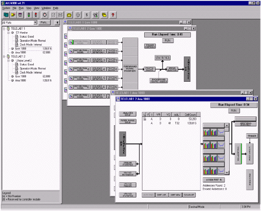
Figure 1. Adtech AX / 4000 software interface
When changing UTOPIA II settings, users will see the interface shown in Figure 2.
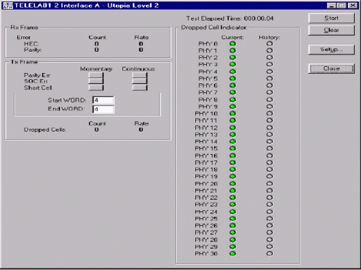
Figure 2. Adtech AX / 4000 software interface of UTOPIA II
Click the SETUP box to access the following functions from the UTOPIA II setup dialog. Figure 3 shows the general mode.
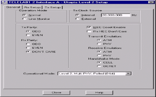
Figure 3. Adtech AX / 4000 software interface for setting UTOPIA II in universal mode
The 'Rx Setup' and 'Tx Setup' in the software interface change the receiving and sending settings. Figures 4 and 5 show the software interface for receiving and sending settings, respectively.
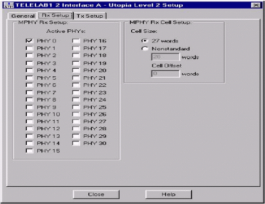
Figure 4. Adtech AX / 4000 software interface for setting UTOPIA II in receive mode
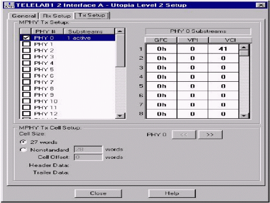
Figure 5. The Adtech AX / 4000 software interface of UTOPIA II is set in the sending mode. The DK2000DK2000 development platform provides 4MB flash memory, which is divided into two. Each block is configured for 512k x 32 and consists of 4 Atmel AT49LV040 with sockets, which is easy to disassemble for external programming. Through the jumper, both flash memory blocks can be configured as boot ROM. The chip select 0 and chip select 1 of the MPC8260 control the flash memory block. The chip selection distribution of each block is configured and selected through jumpers. There is a silk screen on the circuit board to indicate which byte channel the FLASH device is connected to.
To meet the debugging and development requirements, the DK2000 platform provides two debugging connectors. Connector P9 is a standard JTAG / COP interface defined by Motorola to connect to the MPC8260. Connector P20 is a Vision Probe / Vision ICE connector defined by WindRiver.
User software can be downloaded to the on-board SRAM or FLASH through the Vision ICE port or JTAG / COP port. If you use FLASH programming, it is recommended to use FLASH bank 1, FLASH bank 0 contains the default firmware. MPC8260 I / O pin mapping The MPC8260 provides 120 I / O pins that can be configured as dedicated or general purpose I / O. The DK2000 development platform develops I / O functions as much as possible.
Plug the DS2156DK daughter board directly into the DK2000 daughter board connector to complete the connection. Some daughter boards have two connectors, and some have three. The third connector is optional and is used to implement advanced functions (UTOPIA bus, POS-PHY bus, etc.). DK2000 is suitable for both two-connector and three-connector daughter boards, and supports the advanced functions of the third connector. Note that the daughter board does not support hot swapping, and the DK2000 platform can only be connected after the power is turned off. Table 5 lists the pin configuration of the processor MPC8260 in UTOPIA, and how to connect through the daughter board connector.
Table 5. UTOPIA I / O pin assignment
DK101 is a low-cost demonstration motherboard used to evaluate Dallas Semiconductor telecommunications ICs. The IC is mounted on a specially designed daughter board that can be connected to the DK101. DK101 contains a microprocessor, Flash and SRAM-based program memory, various oscillators, auxiliary logic, and RS-232 interface for connecting to the host. The high-performance demo motherboard (DK2000) contains all the auxiliary logic required to fully evaluate the Dallas Semiconductor Telecom daughter board. The processor interface of DK2000 is suitable for various telecommunication products, which is convenient for prototype design and development. The onboard MPC8260, 64MB RAM, up to 1MB L2-Cache, two 2MB Flash, Fast Ethernet and RS-232 make the DK2000 powerful and very flexible.
Introduction DS2156 has two configurable TDM and UTOPIA II bus interfaces. The UTOPIA II interface has the following characteristics: All or part of DS1 / E1, the bit rate is a multiple of 64kbps Unchannelized E1 Complies with the specifications of the ATM Forum for DS1 and E1 carrying ATM UTOPIA II to ATM layer interface can be configured below the UTOPIA address physical layer interface Receive DS1 / E1 data stream clock data in one of the two ways, frame gap indication data position gapped clock loopback diagnosis transmit FIFO depth can be configured to 2, 3 or 4 cells optional single-bit HEC error insertion insertion integration Setting the cell loss indication (LCD) and optional interrupt receiving direction FIFO overflow interrupt DK101 is a low-cost demonstration motherboard used to evaluate Dallas Semiconductor communication ICs. The IC is mounted on a specially designed daughter board that can be connected to the DK101. DK101 contains a microprocessor, Flash and SRAM-based program memory, various oscillators, auxiliary logic, and RS-232 interface for connecting to the host. The processor runs general-purpose firmware, and reads and writes the daughter board through the host demonstration software.
The high-performance demo motherboard (DK2000) contains all the auxiliary logic required to fully evaluate the Dallas Semiconductor Telecom daughter board. The processor interface of DK2000 is suitable for various telecommunication products, which is convenient for prototype design and development. The onboard MPC8260, 64MB RAM, up to 1MB L2-Cache, two 2MB Flash, Fast Ethernet and RS-232 make the DK2000 powerful and very flexible. DK2000 provides processor bus interface, TDM and UTOPIA interfaces for four daughter boards through three 50-line high-density daughter board connectors. DS2156 UTOPIA hardware DS2156 provides user selectable TDM or UTOPIA backplane bus. When UTOPIA II works, basic TDM signals such as clock, synchronization, and data appear simultaneously in the sending and receiving directions.
In ATM applications, select the UTOPIA II bus interface through the TUSEL pin. When TUSEL is low, the TDM bus is enabled; when TUSEL is high, the UTOPIA II bus is enabled. The following describes each pin related to the UTOPIA II bus interface.
UR-ADDR0-UR-ADDR4, receive UTOPIA address, (input): ATM layer drives these 5 UTOPIA address buses, select the corresponding UTOPIA port. RX_UTOP_ADDR4 is the MSB and RX_UTOP_ADDR0 is the LSB.
/ UR-ENB, receive UTOPIA enable, (input): This is an active low-level signal driven by the ATM layer, indicating that UR-DATAx and UR-SOC will be sampled at the end of the next cycle.
UR-SOC, receive UTOPIA cell start (output): When UR-DATAx contains the first valid bit of the cell, DS2156 drives the high-level active signal, it is only after / UR-ENB \ is enabled The period and cell transmission are valid.
UR-DATA0-UR-DATA7, receiving UTOPIA data bus (output): After the ATM layer selects a UTOPIA port for cell transmission, the DS2156 drives this data bus. This bus is a tri-state bus, which is only valid in the period after / UR-ENB \ is enabled and when the cell is transferred. UR-DATA7 is the MSB and UR-DATA0 is the LSB.
UR-CLAV, available for receiving UTOPIA cells (output): if the polled port can transmit a complete cell to the ATM layer, the active high signal is valid. If UR-ADDRx does not match any UTOPIA port address, this signal enters tristate through the control line detailed below. UR-CLAV0 can be multiplexed with 1CLAV to implement polling mode, and at the same time it can implement direct state mode.
UR-CLK, receiving UTOPIA clock (input): receiving UTOPIA bus clock.
UT-ADDR0-UT-ADDR4, send UTOPIA address (input): ATM layer drives this bus, poll and select the appropriate UTOPIA port. UT-ADDR4 is MSB, UT-ADDR0 is LSB.
/ UT-ENB, send UTOPIA enable (input): In the period of UT-DATAx containing valid cells, the ATM layer outputs this low-level effective signal.
UT-SOC, start of sending UTOPIA cell (input): When UT-DATAx contains the first valid byte of the cell, the ATM layer outputs this high-level active signal.
UT-DATA0-UT-DATA7, send UTOPIA data bus (input): 8Bit actual data transmitted by the ATM layer to one of the selected ports. UT-DATA7 is the MSB and UT-DATA0 is the LSB.
UT-CLAV, sending UTOPIA cells is available (output): If the DS2156 has enough space to receive a complete cell at the ATM layer, the DS2156 outputs the active high signal. If UT-ADDRx does not match any UTOPIA port address, this signal enters tristate through the control line detailed below. UT-CLAV0 can be multiplexed with 1CLAV to implement polling mode, and at the same time it can implement direct state mode.
UT-2CLAV, sending UTOPIA 2 cells is available (output): DS2156 outputs this high-level active signal, indicating that the sending end can accommodate two cells. UT-2CLAV0 can be multiplexed with 1CLAV, and port 0 can implement direct state mode. The timing of this signal is the same as UT-CLAV. This bus is not a tri-state bus.
UT-UTDO, UTOPIA send data output (output): the data before entering the send formatter. Update on the rising edge of TCLK. This output is generally connected to TDATA.
UT-CLK, send UTOPIA clock (input): send UTOPIA bus clock. UTPOIA-The UTOPIA interface of the backplane interface DS2156 will send ATM cells mapped to DS1 / E1 frames according to ATM Forum specifications af-phy-0016.000 and af-phy-0064.000, and receive cells in the same mapping manner. On the receiving side, the ATM cell boundary is determined according to the cell description mechanism of ITU-T I.432. The ATM layer is synonymous with the system side, and refers to the UTOPIA II interface of the DS2156. UTPOIA-Sending operation The interface of DS2156 and ATM layer fully complies with the UTOPIA Level 2 specification of ATM Forum, and supports both direct state and multiplexing mode with 1CLAV. The DS2156 can be configured to use one of the 0 to 31 addresses as its UTOPIA port address to provide 4 cell buffers for cell rate adaptation.
The transmit FIFO depth can be set to 2, 3 or 4 cells. When the port being polled can receive cells, the DS2156 generates a cell available signal for the port. In addition, the DS2156 can output an indication of 2 cell availability for each port. The DS2156 uses UT-SOC (Start of Transmit UTOPIA Cell) to detect the first byte of the cell. If a pseudo UT-SOC occurs during cell transmission, the DS2156 locates the last UT-SOC and ignores the incomplete cell UTPOIA in the FIFO-Receive operation The DS2156 receive interface fully complies with the UTOPIA Level 2 specification of the ATM Forum. The DS2156 can be configured to use one of the address ranges 0 to 7, 8 to 15, 16 to 23, and 24 to 32 as the UTOPIA port address. For direct status polling, the address range can be one of 0 to 3, 8 to 11, 16 to 19, and 24 to 27.
If the receive FIFO is not empty, the cell available signal is output. This signal should be updated according to the empty state of the receive FIFO one clock cycle after the port completes the cell transmission. During this clock cycle, the cell available signal of the port is in an unavailable state. Between two cells continuously transmitted on the same UTOPIA port, the DS2156 requires at least one clock delay to update the internal cell pointer. DS2156DK I / O pins are connected to Adtech AX / 4000 by mapping. Table 1 lists how to connect DS2156DK and Adtech AX / 4000 broadband test system to test the DS2156 UTOPIA II bus.
Table 1. I / O pin mapping and Adtech AX / 4000 connection
| Adtech Tx Pin Numbers | Adtech Tx Pin Names | DS2156DK Pin Names | Adtech Rx Pin Numbers | Adtech Rx Pin Names | DS2156DK Pin Names |
| 1 | TXDATA_0 | TNEGI | 1 | RXDATA_0 | RLINK |
| 2 | TXDATA_1 | TCLKI | 2 | RXDATA_1 | RLCLK |
| 3 | TXDATA_2 | TCLKO | 3 | RXDATA_2 | RPOSI |
| 4 | TXDATA_3 | TNEGO | 4 | RXDATA_3 | RNEGI |
| 6 | TXDATA_4 | TPOSO | 6 | RXDATA_4 | RCLKI |
| 7 | TXDATA_5 | TSER | 7 | RXDATA_5 | RCLKO |
| 8 | TXDATA_6 | TSIG | 8 | RXDATA_6 | RNEGO |
| 9 | TXDATA_7 | TSYSCLK | 9 | RXDATA_7 | RPOSO |
| 5,10,20,25,30 | GND | GND | 5,10,20,40,45 | GND | GND |
| twenty two | TXSOC | UOP0 | twenty two | RXSOC | RCHBLK |
| twenty three | TXADDR0 | UOP3 | 37 | RXADDR0 | RCHCLK |
| twenty four | TXADDR1 | TCHBLK | 38 | RXADDR1 | RSIGF |
| 26 | TXADDR2 | TLCLK | 39 | RXADDR2 | RSIG |
| 27 | TXADDR3 | TLINK | 41 | RXADDR3 | RMSYNC |
| 28 | TXADDR4 | TPOSI | 42 | RXADDR4 | RFSYNC |
| 29 | TXCLAV0 | LIUC | 43 | RXCLAV0 | RSER |
| 34 | TXENABLE | UOP1 | 48 | RXENB | BPCLK |
| 36 | UT_CLK | TSSYNC | 49 | UR_CLK | TCHCLK |
After configuring the registers, the user needs to trigger the MSTREG.URST bit to reset the UTOPIA II core.
Table 2. UTOPIA II settings, register settings for daughter board CPLD
| Name | Value | Name | Value | |
| SWITCH 1 | 0x0F | SWITCH 4 | 0x0F | |
| SWITCH 2 | 0x03 | LEVELS | 0x07 | |
| SWITCH 3 | 0x0F |
The register settings in Table 3 are used to configure the DS2156 to work in E1 mode.
Table 3. UTOPIA II settings, register settings for E1 configuration
| Name | Value | Name | Value | |
| MSTREG | 0x02 | LBCR | 0x00 | |
| E1RCR1 | 0x68 | TAF | 0x9B | |
| E1RCR2 | 0x00 | TNAF | 0xC0 | |
| E1TCR1 | 0x15 | LIC1 | 0x11 | |
| E1TCR2 | 0x00 | LIC2 | 0x90 | |
| CCR1 | 0x00 | LIC3 | 0x00 | |
| CCR4 | 0x00 | LIC4 | 0x00 | |
| IOCR1 | 0x00 | |||
| IOCR2 | 0x00 |
The register settings in Table 4 are used to configure the DS2156 as UTOPIA II.
Table 4. UTOPIA II settings, register settings during UTOPIA II configuration
| Name | Value | Name | Value | |
| U_TCFR | 0x01 | U_RCR2 | 0x0 | |
| U_tCR1 | 0x05 | U_TIUPB | 0x0 | |
| U_TCR2 | 0x00 | PCPR | 0x22 | |
| U_RCFR | 0x01 | PCDR1-4 | 0x0 | |
| U_RCR1 | 0x01 |
Figure 1 shows the interface that users see when configuring UTOPIA II using Adtech AX / 4000 software.
Figure 1. Adtech AX / 4000 software interface
When changing UTOPIA II settings, users will see the interface shown in Figure 2.
Figure 2. Adtech AX / 4000 software interface of UTOPIA II
Click the SETUP box to access the following functions from the UTOPIA II setup dialog. Figure 3 shows the general mode.
Figure 3. Adtech AX / 4000 software interface for setting UTOPIA II in universal mode
The 'Rx Setup' and 'Tx Setup' in the software interface change the receiving and sending settings. Figures 4 and 5 show the software interface for receiving and sending settings, respectively.
Figure 4. Adtech AX / 4000 software interface for setting UTOPIA II in receive mode
Figure 5. The Adtech AX / 4000 software interface of UTOPIA II is set in the sending mode. The DK2000DK2000 development platform provides 4MB flash memory, which is divided into two. Each block is configured for 512k x 32 and consists of 4 Atmel AT49LV040 with sockets, which is easy to disassemble for external programming. Through the jumper, both flash memory blocks can be configured as boot ROM. The chip select 0 and chip select 1 of the MPC8260 control the flash memory block. The chip selection distribution of each block is configured and selected through jumpers. There is a silk screen on the circuit board to indicate which byte channel the FLASH device is connected to.
To meet the debugging and development requirements, the DK2000 platform provides two debugging connectors. Connector P9 is a standard JTAG / COP interface defined by Motorola to connect to the MPC8260. Connector P20 is a Vision Probe / Vision ICE connector defined by WindRiver.
User software can be downloaded to the on-board SRAM or FLASH through the Vision ICE port or JTAG / COP port. If you use FLASH programming, it is recommended to use FLASH bank 1, FLASH bank 0 contains the default firmware. MPC8260 I / O pin mapping The MPC8260 provides 120 I / O pins that can be configured as dedicated or general purpose I / O. The DK2000 development platform develops I / O functions as much as possible.
Plug the DS2156DK daughter board directly into the DK2000 daughter board connector to complete the connection. Some daughter boards have two connectors, and some have three. The third connector is optional and is used to implement advanced functions (UTOPIA bus, POS-PHY bus, etc.). DK2000 is suitable for both two-connector and three-connector daughter boards, and supports the advanced functions of the third connector. Note that the daughter board does not support hot swapping, and the DK2000 platform can only be connected after the power is turned off. Table 5 lists the pin configuration of the processor MPC8260 in UTOPIA, and how to connect through the daughter board connector.
Table 5. UTOPIA I / O pin assignment
| UTOPIA FuncTIon | Signal Names on the Processor MPC8260 | Pin Numbers on Daughter Card |
| TXENA | PA31 | 16 |
| TXCLAV0 | PA30 | twenty three |
| TXSOC | PA29 | 17 |
| RXENA | PA28 | 42 |
| RXSOC | PA27 | 43 |
| RXCLAV0 | PA26 | 49 |
| TXD0 | PA25 | 13, 17 |
| TXD1 | PA24 | 14 |
| TXD2 | PA23 | 11 |
| TXD3 | PA22 | 12 |
| TXD4 | PA21 | 9 |
| TXD5 | PA20 | 10 |
| TX6 | PA19 | 7 |
| TXCLAV0 | PA30 | twenty three |
| UTOPIA funcTIon | Signal names on the MPC8260 processor | Pin numbers on daughter card |
| TXD7 | PA18 | 8 |
| RXD7 | PA17 | 34 |
| RXD6 | PA16 | 33 |
| RXD5 | PA15 | 36 |
| RXD4 | PA14 | 35 |
| RXD3 | PA13 | 38 |
| RXD2 | PA12 | 37 |
| RXD1 | PA11 | 40 |
| RXD0 | PA10 | 39 |
| TXCLK | PC21 | 18 |
| RXCLK | PC20 | 44 |
| TXADDR0 | PC15 | 6 |
| RXADDR0 | PC14 | 32 |
| TXADDR1 | PC13 | 3 |
| RXADDR1 | PC12 | 29 |
| TXADDR2 / TXCLAV1 | PC7 | 4, 24 |
| RXADDR2 / RXCLAV1 | PC6 | 30, 50 |
| RXADDR3 / RXCLAV2 | PD29 | 27, 47 |
| TXADDR4 / CLAV3 | PD19 | 2, 22 |
| RXADDR4, RXCLAV3 | PA18 | 28, 28 |
| RXPRTY | PD17 | 41 |
| TXADDR3 / TXCLAV2 | PD7 | 1, 21 |
| TXPRTY | ELPD (generated in logic) | 15 |
For the 132kV Oil Immersed Power Transformer, we can produce capacity upto 180MVA. We use the best quality of raw material and advance design software to provide low noise, low losses, low partial discharge and high short-circuit impedance for power transformer.
Our power transformer are widely used in national grid, city grid, rural grid, power plant, industrial and mining enterprise, and petrochemical industry.
132Kv Transformer,132Kv Power Transformer,132Kv Power Transformer With Oltc,132Kv Transformer With Oltc
Hangzhou Qiantang River Electric Group Co., Ltd.(QRE) , https://www.qretransformer.com