As stated by Moore's Law, the density and speed of wafers are growing exponentially for decades. As we all know, this trend of high-speed growth will one day end, but I don't know how much the density and performance of the wafer can reach when this moment comes. With the development of technology, the density of wafers is increasing, and the width of gate oxide layers is decreasing. The multiple effects commonly found in ultra-large-scale integrated circuits (VLSI) become more important and difficult to control. Antenna effect is one of them. . In the past two decades, semiconductor technology has grown rapidly, resulting in products with smaller specifications, higher package density, higher speed circuits, and lower power consumption. This article will discuss antenna effects and solutions to reduce antenna effects.
Antenna effect
Antenna effect or plasma-induced thyristor damage refers to the effect that potentially affects product yield and reliability during MOS wafer processing. Currently, lithography processes use the 'plasma etch' process (or 'dry etch') to fabricate wafers. Plasma is an ionized/active gas used for etching. It provides super mode control (sharp edge/less undercut) and a variety of chemical reactions that are not possible with conventional etching. But everything has two sides, it also brings some side effects, one of which is charging damage.
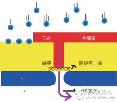
Figure 1: Antenna effect during plasma etching.
Plasma charging damage refers to unintended high field stresses on the MOSFET gate oxide layer during plasma processing. During the plasma etching process, a large amount of charge accumulates on the polycrystalline germanium and metal surfaces. Through the capacitor coupling, a large electric field is formed in the gate oxide layer, resulting in stresses that may damage the oxide layer and change the device threshold voltage (VT). As shown in the figure below, the accumulated static charge is transferred to the gate, passed through the gate oxide layer, and is tunneled by the current.
Obviously, the area of ​​the conductor exposed to the plasma is very important, which determines the static charge accumulation rate and the tunneling current. This is the so-called 'antenna effect'. The area ratio of the conductor of the gate to the oxide layer is the antenna ratio. In general, the antenna ratio can be thought of as a current amplifier that amplifies the density of the tunneling current of the gate oxide layer. For a particular antenna ratio, the higher the plasma density, the greater the tunneling current, which also means higher damage.
Plasma manufacturing includes three procedures. During conductor layer mode etching, the amount of accumulated charge is proportional to the perimeter. In the ashing process, the cumulative charge is proportional to the area. In addition, in the contact etching process, the amount of accumulated charge is proportional to the area of ​​the passing region.
The conventional definition of the antenna ratio (AR) refers to the ratio of the area of ​​the 'antenna' conductor to the area of ​​the gate oxide layer to which it is connected. Conventional theory holds that the degree of reduction in antenna effect is proportional to the antenna ratio (the charging effect of each metal layer is the same). However, the antenna ratio does not actually depend on the antenna effect, but also the layout problem.
The impact of layout on charging damage
The degree of charging damage is a geometric function associated with a very dense gate line antenna. However, charging damage is more susceptible to the electronic masking effect due to etching delay, plasma ashing, oxidative deposition, and plasma induced damage (PID).
Therefore, the new mode of antenna effect needs to consider the etch time factor, as in Equation 1. By controlling the antenna effect by inserting a diode or bridging (wiring), the antenna effect can be more effectively predicted, as shown in Equation 2.
AR= Q/A_Gate .........Formula 1
Where Q refers to the total accumulated charge injected into the gate oxide layer during etching.
V_g=v_(g_max )+αJ/C 2π/(ω) ((P+p))/((A+αa)) .........Form 2
A is the area of ​​the conductive layer, and the capacitor capacity under the plasma current density J is C.
a is the gate area, and the capacitor capacity under the plasma current density J is a
为 is the capacitor ratio
P is the perimeter of the antenna capacitor
p is the perimeter of the gate capacitor
ω is the angular frequency of the plasma power supply
According to the new PID-based mode, the PID does not depend on the AR, but the ratio of the antenna capacitor to the gate capacitor can be a good indicator of the PID. The PID depends on the frequency of the plasma power supply. When the oxide layer is "4nm, the PID will become insensitive to the stress current. Increasing the dielectric constant of the gate without increasing J increases the PID.
Design solutions to reduce antenna effects
The antenna effects of the wafer can be reduced by several design solutions. For example, in the jumper method, the antenna with the antenna effect is disconnected by inserting a jumper, and is routed to the upper metal layer until the last metal layer is etched, and all the etched metal is connected to the gate.
Virtual transistors add additional gates to reduce the capacitor ratio. PFETs are more sensitive than NFETs, but have the problem of reverse antenna effects. The method of adding an embedded protection diode is to connect the reverse biased diode to the gate in the transistor (the diode does not affect the function during normal circuit operation). In addition, the diode is inserted after layout and routing. This method only connects the diode to the metal layer that is subjected to the antenna effect.
A diode protects all input ports connected to the same output port. The two most important ways to eliminate the antenna effect are the jumper method and the insertion of the diode. Next, we will discuss these two methods in detail. The jumper method is the most effective way to respond to antenna effects. Plugging in the diodes solves other antenna problems.
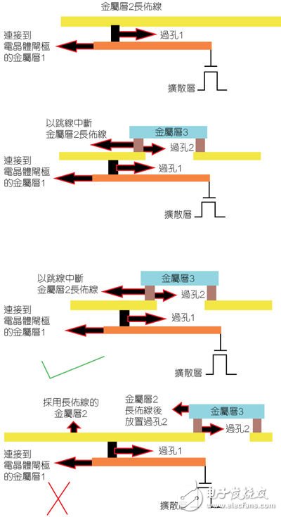
Figure 3: Schematic diagram of the jumper method to reduce antenna effects.
Jumper method
The jumper is to disconnect the metal layer with the antenna effect, connect to other metal layers through the via, and finally return to the current layer. As shown in the figure below, the jumper method divides the long antenna into short antennas, reducing the area of ​​the cable connected to the gate input, thus reducing the accumulated charge.
It is worth noting that the placement of jumpers is important. The jumper must be placed in a position that reduces the length of the wiring. As shown in the figure, in the two pictures, the input and output pins have the same length of spacing, but the jumper position is slightly different. The circuit in the first picture is not affected by the antenna effect, while the circuit in the second picture is affected by the antenna effect.
It can be clearly seen from this example that the use of jumpers (also known as 'bridges') avoids antenna effects. The jumper disconnects the metal layer with the antenna effect, transmits the static charge through the via to the higher metal layer, and then back to the current layer. In the metallization process, in addition to the highest level, the pins are connected to a small cable area to avoid any antenna problems below this layer.
Insert diode
As shown, inserting a diode next to the logic gate input pin provides a charge bleed path for the underlying circuitry, so the accumulated charge does not pose a threat to the gate. The use of a diode provides a charge bleed path for additional ions that are concentrated on the metal layer by the substrate.
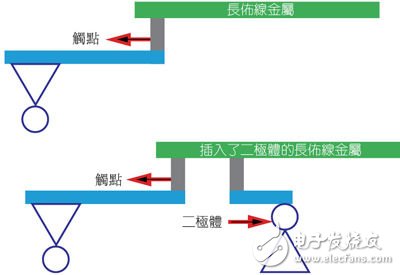
Figure 4: Insert a jumper around the gate.
However, inserting the diode increases the input load of the logic gate, thus increasing the circuit cell area and affecting the timing. In addition, spaces where space is small are not suitable for insertion of diodes.
to sum up
During the fabrication of the wafer, a large amount of electrostatic charge is accumulated thereon due to the exposure of the metal layer. The amount of charge depends on many reasons. From the perspective of the antenna, the amount of charge depends on the exposed area of ​​the metal. The larger the area exposed by the metal, the more charge is accumulated. The substrate is at the bottom and is connected to the fabrication component, thus creating a voltage gradient in the gate oxide layer. When this gradient becomes large enough, it will be released by an explosive discharge (ie 'lightning'). This problem has a very large impact on the small technology field, because the damage caused by the charge discharge may affect the entire gate.
Since the method of expressing the antenna ratio is not uniform, the antenna rule check is different for each process technology. Inserting a reverse biased diode next to the gate that needs to be protected can protect the circuit from antenna effects. During normal execution of the wafer, the reverse biased diode prevents electrons from flowing between the circuit and the diode and prevents electrons from flowing to the wafer substrate.
However, during the manufacturing process, the charge on the circuit will accumulate at a point where the voltage will exceed its tolerance - the voltage is higher than the normal voltage of the circuit, but lower than the expected electrostatic discharge voltage in the gate. . When this happens, the diodes allow electrons to flow from the circuit to the substrate, thus mitigating the charge accumulated in the circuit. This is a non-destructive process, and the circuit can be discharged multiple times through the diode during the manufacturing process.
Another way to avoid antenna effects is to 'cut' (ie, 'jumper') by changing the metal layer. When the metal layer is fabricated, a large metal layer on one side is no longer electrically connected to the gate, so no antenna effect is produced. When connected by a higher-grade metal 'bridge', the conductor surface is no longer exposed and therefore does not collect free charge, thus avoiding antenna effects.
Bitmain Antminer Asic Miner:Bitmain Antminer Z15,Bitmain Antminer Z9 Mini,Bitmain Antminer Z9,Bitmain Antminer Z11
Bitmain is the world's leading digital currency mining machine manufacturer. Its brand ANTMINER has maintained a long-term technological and market dominance in the industry, with customers covering more than 100 countries and regions. The company has subsidiaries in China, the United States, Singapore, Malaysia, Kazakhstan and other places.
Bitmain has a unique computing power efficiency ratio technology to provide the global blockchain network with outstanding computing power infrastructure and solutions. Since its establishment in 2013, ANTMINER BTC mining machine single computing power has increased by three orders of magnitude, while computing power efficiency ratio has decreased by two orders of magnitude. Bitmain's vision is to make the digital world a better place for mankind.
Bitmain Antminer Asic Miner,Z15 bitmain antminer,Z11 Antminer Bitmain,zcash miner,zec mining machine
Shenzhen YLHM Technology Co., Ltd. , https://www.sggminer.com