DRAM (Dynamic Random Access Memory) is particularly attractive to designers because it provides a wide range of performance for storage system designs in a variety of computer and embedded systems. This article outlines the concept of DRAM and introduces SDRAM, DDR SDRAM, DDR2 SDRAM, DDR3 SDRAM, DDR4 SDRAM, LPDDR, GDDR.
DRAMOne advantage of DRAM over other memory types is that it can be implemented with fewer circuits per memory cell on the IC (integrated circuit). The memory cells of a DRAM are based on the charge stored on the capacitor. A typical DRAM cell is fabricated using one capacitor and one or three FETs (Field Effect Transistors). A typical SRAM (Static Random Access Memory) memory cell takes six FET devices, reducing the number of memory cells per IC for the same size. Compared to DRAM, SRAM is easier to use, easier to interface, and faster to access data.
The DRAM core structure consists of multiple memory cells divided into two-dimensional arrays of rows and columns (see Figure 1). Accessing the memory unit requires two steps. Look for the address of a row first, then look for the address of a particular column in the selected row. In other words, the entire row is first read inside the DRAM IC, and then the column address selects which column of the row the DRAM IC I/O pin needs to read or write.
DRAM reads are destructive, that is, data in a memory cell row is corrupted during a read operation. Therefore, it is necessary to write the row data back to the same line at the end of the read or write operation on the line. This operation is called pre-charging and is the last operation on the line. You must do this before you can access the new row, which is called closing the open row.
Analysis of computer memory access shows that the most common type of memory access is the memory address of the read order. This is reasonable because reading computer instructions is generally more common than reading or writing data. In addition, most instruction reads are performed sequentially in memory until an instruction branch occurs or jumps to a subroutine.
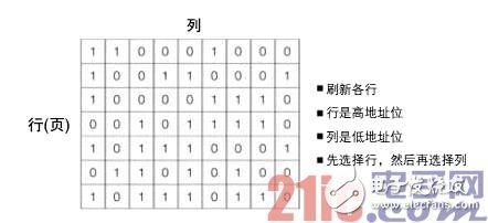
Figure 1. DRAMs Memory cells are divided into two-dimensional arrays of rows and columns.
A row of DRAM is called a memory page. Once a row is opened, you can access multiple sequential or different column addresses in that row. This improves memory access speed and reduces memory latency because it does not have to resend row addresses to DRAM when accessing memory cells in the same memory page. As a result, the row address is the high order address bit of the computer and the column address is the low order address bit. Since the row and column addresses are sent at different times, the row and column addresses are multiplexed onto the same DRAM pins to reduce the number, cost, and size of the package pins. In general, the row address size is larger than the column address because the power used is related to the number of columns.
Earlier RAMs had control signals such as RAS# (row address select low active) and CAS# (column address select low active) to select the row and column addressing operations performed. Other DRAM control signals include WE# (write enable low active) for selecting write or read operations, CS# (chip select low active) for selecting DRAM, and OE# (output enable low active). Early DRAMs had asynchronous control signals and various timing specifications covering their sequence and time relationships to determine DRAM operating modes.
The early DRAM read cycle has four steps. In the first step, RAS# and the row address on the address bus go low. In the second step, the CAS# and the column address on the address bus go low. In the third step, OE# goes low and the read data appears on the DQ data pin. When data is provided on the DQ pin, the time from the third step of the first step is called the delay. The final step is RAS#, CAS# and OE# go high (inactive), waiting for the internal precharge operation to complete the row data recovery after destructive reading. The time from the first step to the end of the last step is the memory cycle time. The signal timing of the above signals is related to the edge order and is asynchronous. These early DRAMs did not have synchronous clock operations.
The DRAM memory unit must be refreshed to avoid losing data content. This requires the capacitor to be refreshed before the charge is lost. The refresh memory is the responsibility of the memory controller, and the refresh time indicator varies depending on the DRAM memory. The memory controller performs a RAS# loop on the row address and refreshes it. At the end of the RAS# only cycle, a precharge operation is performed to restore the row data addressed only in the RAS# loop. In general, the memory controller has a row counter that sequentially generates all the row addresses required for the RAS# refresh cycle only.
There are two refresh strategies (see Figure 2). The first policy memory controller sequentially refreshes all rows in the refresh cycle burst and then returns memory control back to the processor for normal operation. The next refresh operation burst occurs before the maximum refresh time is reached. The second refresh strategy is that the memory controller operates the interlaced refresh cycle with normal processor memory. This refresh method expands the refresh cycle during the maximum refresh time.
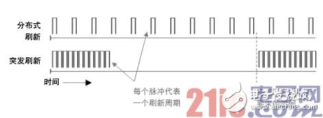
Figure 2. DRAM refresh implementations include distributed refresh and burst refresh.
Early DRAM evolution and implementation of refresh counters on DRAM ICs, processing the row address generated by the sequence. Inside the DRAM IC, the refresh counter is the multiplexer input that controls the memory array row address. The other multiplexer inputs the row address from the external address input pin. This internal refresh counter does not require an external refresh counter circuit in the memory controller. Some DRAMs support a CAS# before the RAS# cycle to initiate a refresh cycle using internally generated row addresses.
SDRAMThe asynchronous operation of DRAM brings many design challenges when it comes to interfacing to a synchronous processor.
SDRAM (Synchronous DRAM) is designed to synchronize DRAM operations to the rest of the computer system without the need to define all memory modes of operation based on CE# (chip startup activity low), RAS#, CAS#, and WE# edge transition sequences.
SDRAM adds the concept of clock signals and memory commands. The type of memory command depends on the CE#, RAS#, CAS#, and WE# signal states on the rising edge of the SDRAM clock. The product data describes the memory commands in tabular form according to the CE#, RAS#, CAS# and WE# signal states.
For example, the AcTIvate (Activate) command sends a row address to SDRAM, opening a row (page) of memory. This is followed by a Deselect (inverse selection) command sequence that satisfies the timing requirements before sending a Read or Write command to the column address. Once the line (page) of memory is opened using the AcTIvate command, multiple Read and Write commands can be run on that line (page) of memory. A Precharge command is required to close the line before another line can be opened.
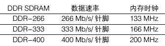
Table 1. DDR SDRAM data rates and clock speeds.
DDR SDRAMDDR (Double Data Rate) SDRAM improves memory data rate performance by increasing clock rates, burst data, and transferring two data bits per clock cycle (see Table 1). DDR SDRAM bursts multiple memory locations in one read command or one write command. The read memory operation must send an AcTIvate command followed by a Read command. After a delay, the memory responds to a burst consisting of two, four, or eight memory locations at a data rate of two memory locations per clock cycle. Therefore, four memory locations are read from two consecutive clock cycles, or four memory locations are written in two consecutive clock cycles.
DDR SDRAM has multiple memory banks that provide multiple interlaced memory accesses to increase memory bandwidth. A memory module is a memory array, two memory modules are two memory arrays, four memory modules are four memory arrays, and so on (see Figure 3). Four memory banks require two bits for the memory bank address (BA0 and BA1).
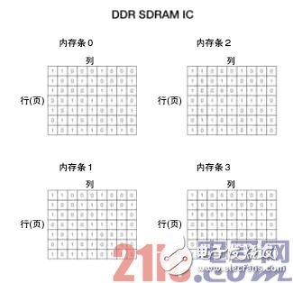
Figure 3. Multiple memory banks in DDR SDRAM improve access flexibility and performance.
For example, a DDR SDRAM with four memory banks works as follows. First, the AcTIvate command opens a line in the first memory stick. The second Activate command opens a line in the second memory stick. Now, you can send any combination of Read or Write commands to the first or second memory bank of the open row. At the end of the Read and Write operations on the memory bank, the Precharge command closes the line, and the memory module is ready for the Activate command to open a new line.
Note that the power required by DDR SDRAM is related to the number of memory banks that open the row. The more rows that are opened, the higher the power required, the larger the row size, and the higher the power required. Therefore, for low-power applications, only one row should be opened in each memory bank at a time, rather than multiple memory banks that open rows at a time.
Continuous memory words in interlaced contiguous memory banks are supported when the memory bank address bits are connected to lower order address bits in the memory system. When the memory bank address bits are connected to higher-order addresses in the memory system, the contiguous memory words are in the same memory bank.
DDR2 SDRAMDDR2 SDRAM has many improvements over DDR SDRAM. The DDR2 SDRAM has a higher clock rate, which increases the memory data rate (see Table 2). As clock rates increase, signal integrity becomes more and more important for reliable memory operation. As the clock rate increases, the signal traces on the board become transmission lines, and proper layout and termination at the end of the signal line becomes more important.
The termination of the address, clock, and command signals is relatively straightforward because the signals are unidirectional and terminated on the board. Data signals and data strobes are bidirectional. The memory controller center drives these signals during write operations, and DDR2 SDRAM drives these signals during read operations. Multiple DDR2 SDRAMs are connected to the same data signal and data strobe for added complexity. Multiple DDR2 SDRAMs can be located on the same DIMM in the memory system or on different DIMMs in the memory system. As a result, data and data strobe drivers and receivers are constantly changing, depending on the read/write operation and which DDR2 SDRAM is being accessed.
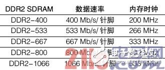
Table 2. DDR2 SDRAM data rates and clock speeds.
DDR2SDRAM improves signal by providing ODT (in-chip termination) and providing ODT signals for on-chip termination and programming of on-chip termination values ​​(75 ohms, 150 ohms, etc.) using DDR2 SDRAM extended mode registers Integrity.
On-chip termination size and operation are controlled by the memory controller hub, depending on the location of the DDR2 SDRAM DIMM and the type of memory operation (read or write). ODT operation improves signal integrity by creating larger eye diagrams for data valid windows, increasing voltage margin, increasing slew rate, reducing overshoot, and reducing ISI (intersymbol interference).
DDR2 SDRAM operates at 1.8V, reducing the power of the memory system, which is 72% of the 2.5V power of DDR SDRAM. In some implementations, the number of columns in the row has decreased, reducing power when the row is activated for reading or writing.
Another advantage of lowering the operating voltage is the reduced logic voltage swing. At the same slew rate, a falling voltage swing increases the logic conversion speed and supports a faster clock rate. In addition, data strobes can be programmed as differential signals. Using differential data strobe signals reduces noise, crosstalk, dynamic power, and EMI (electromagnetic interference), increasing noise margin. The differential or single-ended data strobe operation is configured with a DDR2 SDRAM extended mode register.
A new feature introduced by DDR2 SDRAM is the additional latency, which allows the memory controller hub to send Read and Write commands more flexibly and faster after the Activate command. This optimizes memory throughput and is configured by additional latency programming using the DDR2 SDRAM extended mode register. DDR2 SDRAM uses eight memory banks to improve the data bandwidth of 1Gb and 2GbDDR2 SDRAM. By interleaving different memory stick operations, eight memory sticks increase the flexibility of accessing large memory DDR 2 SDRAM. In addition, for large memory, DDR2 SDRAM supports burst lengths of up to eight memory banks.
DDR3 SDRAMDDR3 SDRAM is a performance-enhancing version that enhances SDRAM technology starting at 800 Mb/s, the highest data rate supported by most DDR2 SDRAMs. DDR3 SDRAM supports six data rates and clock speeds (see Table 3). DDR3-800/1066/1333SDRAM was put into use in 2007, DDR3-1600/1866SDRAM is expected to be put into use in 2008, and DDR3-2133SDRAM is expected to be put into use in 2009.
DDR3-1066 SDRAM consumes less power than DDR2-800 SDRAM because DDR3 SDRAM operates at 1.5 V, which is 83% of DDR2 SDRAM, and DDR2 SDRAM operates at 1.8 V. In addition, the DDR3 SDRAM data DQ driver has an impedance of 34 ohms and the DDR2 SDRAM has a low impedance of 18 ohms.
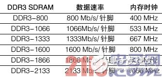
Table 3. Estimated DDR3 SDRAM data rates and clock speeds.
DDR3 SDRAM will start with 512 Mb of memory and will grow to 8 Gb of memory in the future. Like DDR2 SDRAM, DDR3 SDRAM data output configurations include x4, x8, and x16. DDR3 SDRAM has 8 memory sticks, and DDR2 SDRAM has 4 or 8 memory sticks depending on the size of the memory.
Both DDR2 and DDR3 SDRAM have four mode registers. DDR2 defines the first two mode registers, and the other two mode registers are reserved for future use. DDR3 uses all four mode registers. An important difference is that the DDR2 mode register specifies the CAS latency for read operations, and the write latency is 1 minus the mode register read latency setting. The DDR3 mode register is unique to the CAS read latency and write latency settings.
DDR3 SDRAM uses an 8n prefetch architecture to transmit 8 data words in 4 clock cycles. DDR2 SDRAM uses a 4n prefetch architecture to transfer 4 data words in 2 clock cycles.
The DDR3 SDRAM mode register can be programmed to support flight abrupt changes, which shortens the transfer of 8 data words to transfer 4 data words, which is achieved by setting address line 12 low during a read or write command. The flight mutation is conceptually similar to the read and write auto-precharge function of address line 10 in DDR2 and DDR3 SDRAM.
Another DDR3 SDRAM property worth mentioning is the differential data strobe signal DQS, which can be programmed to single-ended or differential by the mode register. DDR3 SDRAM also has a new pin, which is the active low asynchronous RESET# pin, which improves system stability by placing the SDRAM in a known state regardless of the current state. DDR3 SDRAM uses the same FBGA package type as DDR2 SDRAM.
DDR3 DIMMs provide termination for commands, clocks, and addresses on DIMMs. The memory system with DDR2 DIMMs terminates the commands, clocks, and addresses on the motherboard. The DDR3 DIMM termination on the DIMM supports the flight topology. Each command, clock, and address pin on the SDRAM is connected to a trace that is then terminated at the trace end of the DIMM. This improves signal integrity and runs faster than the DDR2 DIMM tree structure.
The flight topology introduces a new DDR3 SDRAM write level function for the memory controller, taking into account the timing offset between the clock CK and the data strobe signal DQS during writing. DDR3 DIMMs are primarily different from DDR2 DIMMs, preventing the wrong DIMMs from being inserted into the motherboard.
DDR4 SDRAMDDR4 SDRAM has been launched and is expected to be released in 2012. The goal is to run these new memory chips on a 1.2V or lower power supply while achieving data transfer speeds of more than 2 million per second.
GDDR and LPDDROther DDR variants, such as GDDR (Graphics DDR) and LPDDR (Low Power DDR), are also growing in the industry.
GDDR is a graphics card dedicated storage technology, currently has four variants: GDDR2, GDDR3, GDDR4 and GDDR5. GDDR technology is very similar to traditional DDR SDRAM, but with different power requirements. It reduces power requirements to simplify cooling and provide higher performance memory modules. GDDR is also designed to better handle processing graphics requirements.
With a clock rate of 166 MHz, LPDDR is becoming more popular in portable consumer electronics where low power is required. LPDDR2 improves energy efficiency with a minimum operating voltage of 1.2V and a clock speed of 100-533 MHz.
Guangzhou Yunge Tianhong Electronic Technology Co., Ltd , https://www.e-cigarettesfactory.com