Current industrial systems are evolving toward electrification, and as voltage levels continue to rise and peak currents increase to hundreds of amps, the time to activate these systems must be as fast as possible, while the performance of in-vehicle systems continues to increase.
Increasing reliability has prompted manufacturers to reduce mechanical systems and add solid-state systems, including protection circuits for power supplies, loads, and solid-state power devices... So how do you solve the electrical design problems in automotive and industrial applications?

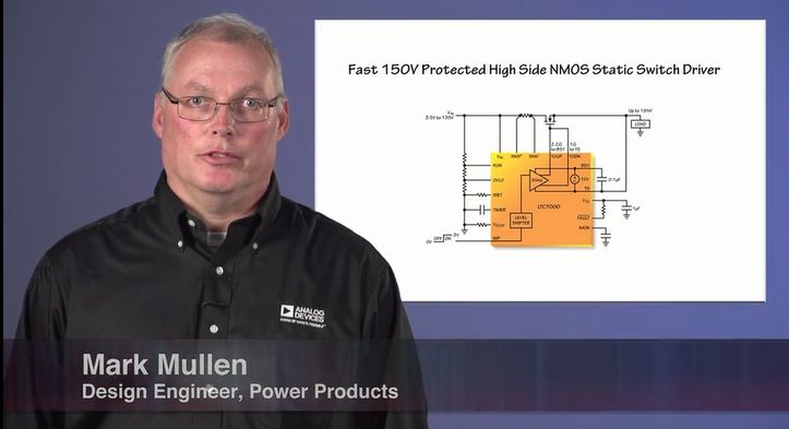
 The Savior is coming - high voltage side drive solution
 Mark Mullen, design engineer for the ADI Power Products Group, shared a LCT7000-protected high-voltage side driver solution for these issues .
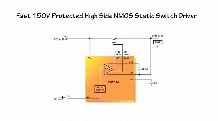
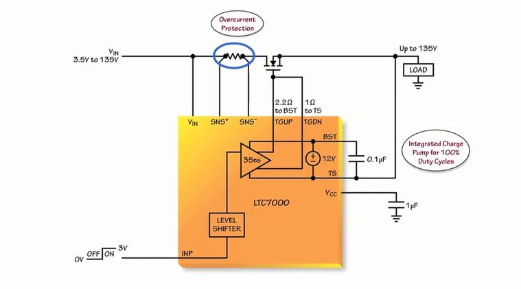
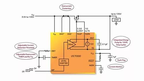
The LTC7000 is a fast, high-side N-channel MOSFET gate driver that accepts a low-voltage digital input signal that is referenced to ground and fully turns on or off one of its drains above ground potential with a propagation delay of 35ns. High-voltage side N-channel MOSFET up to 135V. The fast rise and fall times of 13ns (when driving a 1000pF load) minimize switching losses. Its internal charge pump fully enhances an external N-channel MOSFET switch, allowing it to remain on indefinitely.
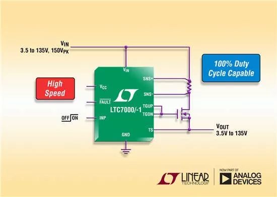
It also has a powerful 1Ω gate driver that drives large gate capacitance MOSFETs with very short conversion times. This overcurrent trip function is ideal for high frequency switching and static switching applications. Together with protection features such as fault marking, undervoltage lockout and overvoltage lockout, it can be found to be very useful in the industrial and automotive markets, such as static switch drivers, load and power switch drivers and relay replacement products. Next we will talk about the characteristics of the LTC7000~
Features 1, low latency, fast
The LTC7000 receives a low-voltage digital signal referenced to ground on the INP pin, shifting the signal level up to VIN. It also controls the on-chip low-impedance pull-up and pull-down devices to quickly turn on or determine a high-side N-channel MOSFET whose drain can rise above 135V. The propagation delay from a low-voltage INP signal to a fully-enhanced or fully-off N-channel MOSFET is about 35ns, which also contributes to many applications.
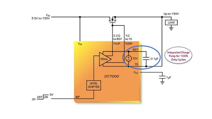
Features 2, low power loss, strong stability
The floating supply between the BOOST and TS pins is internally regulated to 12V, which reduces the power loss caused by the on-resistance of the external MOSFET. A powerful output device maintains the external MOSFET in a state controlled by a low voltage INP signal, even when high voltage and high frequency transients are coupled back from the power MOSFET to the driver circuit.
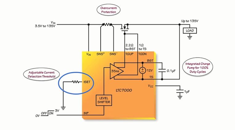
If the application current jump is required to be 10A, only 300mW (maximum) is dissipated in the sense resistor. For added flexibility, the current sense threshold voltage can be selectively adjusted between 20mV and 75mV by changing the voltage on the ISET pin.
Features three, adjustable current limit
The voltage on the ISET pin is divided by 20 to set the current detection threshold. The ISET pin will drain a 10μA current, so simply place a resistor between the ISET pin and ground to adjust the current sense threshold. If the ISET pin is floating, the current sense threshold defaults to 30mV. If the ISET pin is grounded, the current detection threshold is 20mV.
Because the LTC7000 also has a TIMER pin, the overcurrent condition does not immediately turn off the external MOSFET. Connect a capacitor between the TIMER pin and ground to set the delay period before the external MOSFET is turned off in the event of an overcurrent fault. The turn-off delay period can be set to a minimum of 1.4μs (if TIMER is cited) Open circuit) To the tens or hundreds of ms (if the capacitor is μF), the same capacitor placed on the TIMER pin is also responsible for setting a cooling cycle.
After this cooling cycle, the internal circuit will automatically attempt to re-turn on the external MOSFET with a retry duty cycle of approximately 0.06%. Therefore, the appropriate overcurrent trip point and TIMER capacitor should be chosen to protect the external MOSFET by holding the MOSFET in the safe operating area specified in the MOSFET product manual.
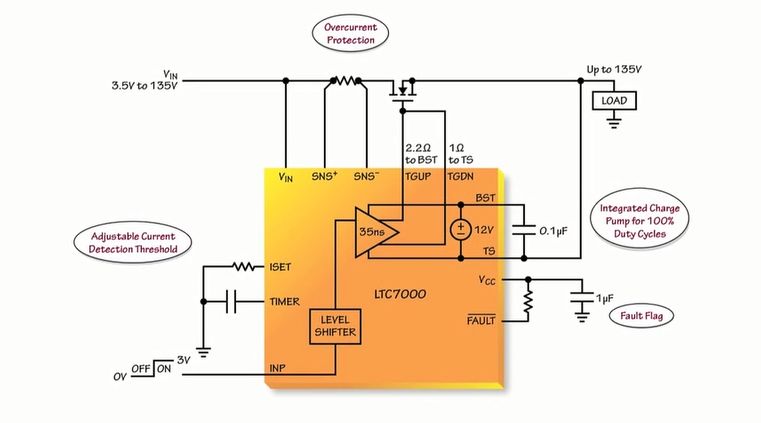
And if an overcurrent fault condition is detected, then pull an open-drain FAULT pin low. This FAULT pin is held low until the fault condition is cleared and the external MOSFET turns back on.
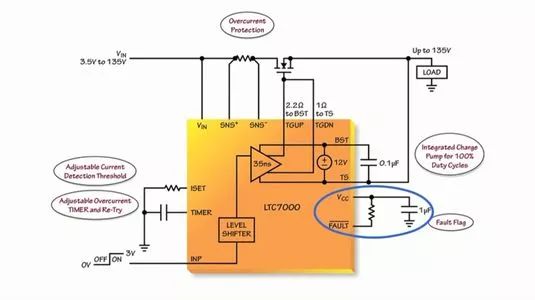
Configuring the LTC7000 to perform latch-up instead of automatic retry can be accomplished by adding a 100kΩ resistor in parallel with the TIMER capacitor. The turn-off delay for overcurrent faults will still be set by the TIMER capacitor, but the LTC7000 will not automatically attempt to re-turn on the external MOSFET after an overcurrent fault, and the external MOSFET will not attempt to turn back on until the low voltage INP signal cycles to Low and then return high.
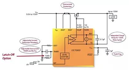
In this configuration, once an overcurrent fault is detected, the open-drain FAULT pin will be pulled low and will remain low until the INP signal cycles low and then returns high.
Feature 4, current monitor output
The average current flowing through the high side detection resistor can be monitored by measuring the voltage on the IMON pin. When the external MOSFET is turned on, the voltage appearing on the IMON pin is the sense voltage, (VSNS+ – VSNS–) x 20. Assuming the sense resistor is 2mΩ, an IMON voltage of 400mV means that 10A of current flows through the sense resistor. The average time of the IMON voltage is approximately 1 MΩ multiplied by any capacitance on the IMON pin. For example, if the capacitance on the IMON pin is 1nF, the average time for the IMON output voltage is approximately 1ms.
Features 5, adjustable input undervoltage and overvoltage lockout
The LTC7000 protects the load from overvoltage and undervoltage conditions on the VIN pin. “A simple resistor divider connected between VIN and ground and tapped to the RUN and OVLO pins will set a valid operating window for the load. When VIN is at the operation set by the RUN and OVLO pins Outside the window, the external MOSFET is turned off and the load is protected from potential damage or failure,†Mark Mullen said.
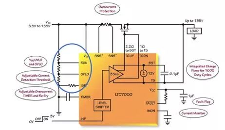
The VCCUV pin also provides undervoltage lockout protection for the VCC supply. The VCC undervoltage lockout threshold can be adjusted between 3.5V and 10.5V by changing the VCCUV pin voltage. A 10μA current flows from the VCCUV pin, so a VCC undervoltage lockout threshold can be adjusted by simply placing a resistor between the VCCUV pin and ground. If the VCCUV pin is floating, the VCC undervoltage lockout threshold defaults to 7V. If the VCCUV pin is grounded, the VCC undervoltage lockout voltage is set to 3.5V. The external MOSFET is turned off when the voltage on the VCC pin is below the undervoltage lockout threshold set by the VCCUV pin.

This shows that as a flexible and rugged device, automotive and industrial manufacturers can improve the performance and reliability of their systems. The LTC7000 's voltage range of up to 135V, built-in protection, powerful drivers, fast turn-on and turn-off time capabilities enable manufacturers to develop systems that add value and reliability to their customers. It is therefore used primarily for static switch drivers, load and power switch drivers, electronic valve drivers, and high frequency, high voltage gate drivers.
Lithium Battery Cr123A,123 Lithium Battery,Cr123A 3V Lithium Battery,Cr123A Lithium Batteries
Jiangmen Hongli Energy Co.ltd , https://www.honglienergy.com