The MAX6954 is a universal display driver that can control multiple discrete, 7-segment, 14-segment, or 16-segment LED displays via a serial port. This application note describes typical applications and configurations for driving 8-bit monochrome, 7-segment LED displays.
For more information about MAX6954, please refer to the MAX6954 data sheet.
Application notes "Quick Start: Using MAX6954 to Drive a 16-Segment LED Display" and "Quick Start: Using MAX6954 to Drive a 14-Segment LED Display" Similar to this article, they explain how to configure the MAX6954 to drive 16- and 14-segment displays, respectively.
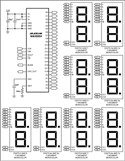
Enlarged display Figure 1. The MAX6954 drives a 7-segment display circuit
A common application of the MAX6954 is to drive up to 16-bit 7-segment monochrome LEDs. This application note guides the user how to connect the MAX6954 to a 7-segment display and how to configure its internal registers to control the display of hexadecimal characters.
The MAX6954 uses a multiplexing technique that alternates the polarity of the driver port to reduce the number of pins. This is different from the standard LED multiplexing connection used separately for the cathode and anode pins of the driver. Application note "Charlieplexing-Reduced Pin-Count LED Display MulTIplexing" discusses this technology. Table 1 is the connection table between MAX6954 and 7-segment display. This table is compatible with the multiplexing configuration of MAX6954 and its built-in font of hexadecimal characters. The letters in Table 1 correspond to the segment identifiers in Figure 2. Figure 1 is a schematic diagram of the MAX6954 driving a 16-bit 7-segment display.
Table 1. Connection table with 16-bit 7-segment display
| Digit | O0 | O1 | O2 | O3 | O4 | O5 | O6 | O7 | O8 | O9 | O10 | O11 | O12 | O13 | O14 | O15 | O16 | O17 | O18 |
| 0, 0a | CC0 | - | 1a | - | 1b | 1c | 1d | 1dp | 1e | 1f | 1g | 2a | 2b | 2c | 2d | 2e | 2f | 2g | 2dp |
| 1, 1a | - | CC1 | 1a | - | 1b | 1c | 1d | 1dp | 1e | 1f | 1g | 2a | 2b | 2c | 2d | 2e | 2f | 2g | 2dp |
| 2, 2a | 1a | - | CC2 | - | 1b | 1c | 1d | 1dp | 1e | 1f | 1g | 2a | 2b | 2c | 2d | 2e | 2f | 2g | 2dp |
| 3, 3a | 1a | - | - | CC3 | 1b | 1c | 1d | 1dp | 1e | 1f | 1g | 2a | 2b | 2c | 2d | 2e | 2f | 2g | 2dp |
| 4, 4a | 1a | - | 1b | 1c | CC4 | - | 1d | 1dp | 1e | 1f | 1g | 2a | 2b | 2c | 2d | 2e | 2f | 2g | 2dp |
| 5, 5a | 1a | - | 1b | 1c | - | CC5 | 1d | 1dp | 1e | 1f | 1g | 2a | 2b | 2c | 2d | 2e | 2f | 2g | 2dp |
| 6, 6a | 1a | - | 1b | 1c | 1d | 1dp | CC6 | - | 1e | 1f | 1g | 2a | 2b | 2c | 2d | 2e | 2f | 2g | 2dp |
| 7, 7a | 1a | - | 1b | 1c | 1d | 1dp | - | CC7 | 1e | 1f | 1g | 2a | 2b | 2c | 2d | 2e | 2f | 2g | 2dp |
After the MAX6954 is connected to the 7-segment display, the display test mode can be used to check the correctness of the connection. The display test mode is not affected by the control and data registers, and lights all segments of the display, but does not change any register contents. Write 0x01 to register 0x07 to start the display test mode. In the test mode, if there is an unlit segment on the display, the connection is incorrect. Write 0x00 to register 0x07 to exit display test mode.
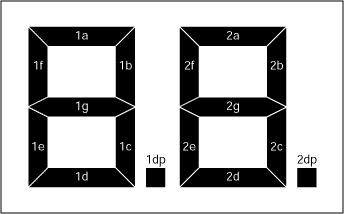
Figure 2. Segment identification of 7-segment display
After completing the connection check, you need to set the MAX6954 register value as required to drive the 7-segment display. Table 2 includes the power-on initial values ​​of some important registers of MAX6954. The MAX6954 is in power-down mode when it is first powered on. Everyone displays blanking, selects a 7-segment font and sets the maximum number of scan digits, that is, eight bits. The MAX6954 can be set to a mode that drives a 7-segment display by writing 0xFF to register 0x0C. The default value of the decoding mode register (0x01) applies to 7-segment displays.
Table 2. MAX6954 register power-on initial state
| REGISTER | POWER-UP CONDITION | ADDRESS (HEX) | REGISTER DATA | |||||||
| D7 | D6 | D5 | D4 | D3 | D2 | D1 | D0 | |||
| Decode Mode | 7-segment font enabled | 0x01 | 1 | 1 | 1 | 1 | 1 | 1 | 1 | 1 |
| Global Intensity | 1/16 (minimum intensity) | 0x02 | X | X | X | X | 0 | 0 | 0 | 0 |
| Scan Limit | Display sixteen 7-segment digits: 0, 1, 2, 3, 4, 5, 6, 7, 0a, 1a, 2a, 3a, 4a, 5a, 6a, 7a | 0x03 | X | X | X | X | X | 1 | 1 | 1 |
| Control Register | Shutdown enabled, blink disabled, blink speed is slow | 0x04 | 0 | 0 | X | X | 0 | 0 | 0 | 0 |
| Display Test | Normal operaTIon (display test disabled) | 0x07 | X | X | X | X | X | X | X | 0 |
| Digit Type | Digits 0 through 7 are 7 segment digits | 0x0C | 0 | 0 | 0 | 0 | 0 | 0 | 0 | 0 |
| Intensity10 | 1/16 (min on), digits 1 and 0 | 0x10 | 0 | 0 | 0 | 0 | 0 | 0 | 0 | 0 |
| Intensity32 | 1/16 (min on), digits 3 and 2 | 0x11 | 0 | 0 | 0 | 0 | 0 | 0 | 0 | 0 |
| Intensity54 | 1/16 (min on), digits 5 and 4 | 0x12 | 0 | 0 | 0 | 0 | 0 | 0 | 0 | 0 |
| Intensity76 | 1/16 (min on), digits 7 and 6 | 0x13 | 0 | 0 | 0 | 0 | 0 | 0 | 0 | 0 |
| Intensity10a | 1/16 (min on), digits 1a and 0a | 0x14 | 0 | 0 | 0 | 0 | 0 | 0 | 0 | 0 |
| Intensity32a | 1/16 (min on), digits 3a and 2a | 0x15 | 0 | 0 | 0 | 0 | 0 | 0 | 0 | 0 |
| Intensity54a | 1/16 (min on), digits 5a and 4a | 0x16 | 0 | 0 | 0 | 0 | 0 | 0 | 0 | 0 |
| Intensity76a | 1/16 (min on), digits 7a and 6a | 0x17 | 0 | 0 | 0 | 0 | 0 | 0 | 0 | 0 |
| Digit 0 | Blank digit, both planes | 0x60 | 0 | 0 | 1 | 0 | 0 | 0 | 0 | 0 |
| Digit 1 | Blank digit, both planes | 0x61 | 0 | 0 | 1 | 0 | 0 | 0 | 0 | 0 |
| Digit 2 | Blank digit, both planes | 0x62 | 0 | 0 | 1 | 0 | 0 | 0 | 0 | 0 |
| Digit 3 | Blank digit, both planes | 0x63 | 0 | 0 | 1 | 0 | 0 | 0 | 0 | 0 |
| Digit 4 | Blank digit, both planes | 0x64 | 0 | 0 | 1 | 0 | 0 | 0 | 0 | 0 |
| Digit 5 | Blank digit, both planes | 0x65 | 0 | 0 | 1 | 0 | 0 | 0 | 0 | 0 |
| Digit 6 | Blank digit, both planes | 0x66 | 0 | 0 | 1 | 0 | 0 | 0 | 0 | 0 |
| Digit 7 | Blank digit, both planes | 0x67 | 0 | 0 | 1 | 0 | 0 | 0 | 0 | 0 |
| Digit 0a | Blank digit, both planes | 0x68 | 0 | 0 | 1 | 0 | 0 | 0 | 0 | 0 |
| Digit 1a | Blank digit, both planes | 0x69 | 0 | 0 | 1 | 0 | 0 | 0 | 0 | 0 |
| Digit 2a | Blank digit, both planes | 0x6A | 0 | 0 | 1 | 0 | 0 | 0 | 0 | 0 |
| Digit 3a | Blank digit, both planes | 0x6B | 0 | 0 | 1 | 0 | 0 | 0 | 0 | 0 |
| Digit 4a | Blank digit, both planes | 0x6C | 0 | 0 | 1 | 0 | 0 | 0 | 0 | 0 |
| Digit 5a | Blank digit, both planes | 0x6D | 0 | 0 | 1 | 0 | 0 | 0 | 0 | 0 |
| Digit 6a | Blank digit, both planes | 0x6E | 0 | 0 | 1 | 0 | 0 | 0 | 0 | 0 |
| Digit 7a | Blank digit, both planes | 0x6F | 0 | 0 | 1 | 0 | 0 | 0 | 0 | 0 |
The configuration register (0x04) is used to set the entry and exit of the shutdown mode, control the blinking function, globally clear the data of each bit, and select whether to control the brightness of each bit globally or individually. The configuration register contains 7 bits (see Table 3). The S bit is used to select power-down mode or normal operating mode (read / write). Bit B is used to select the blinking rate (read / write). The E bit is used to globally enable or disable the flashing function (read / write). The T bit is used to reset the blinking sequence (this data is not stored-transient bit). The R bit is used to globally clear the P0 and P1 two-level registers corresponding to all display bits (this data is not stored-transient bit). The I bit is used to select whether the brightness of each bit is controlled globally or individually (read / write). The P bit is used to return to the current blink timing phase (read-only-writing to this bit will be ignored). Table 3. Configuration register format
| CONFIGURATION REGISTER DATA BIT | DATA BIT LABEL | STATE | FUNCTION |
| D7 | P | 0 | P1 Blink Phase |
| D6 | I | 0 | Intensity for all digits is controlled by one setting in the Global Intensity Register |
| 1 | Intensity for digits is controlled by the individual settings in the Intensity10 through Intensity76a registers. | ||
| D5 | R | 0 | Digit data for both planes P0 and P1 are unaffected |
| 1 | Digit data for both planes P0 and P1 are cleared on the rising edge of active-low CS | ||
| D4 | T | 0 | Blink timing counters are unaffected. |
| 1 | Blink timing counters are reset on the rising edge of active-low CS. | ||
| D3 | E | 0 | Blink function disabled |
| 1 | Blink function enabled | ||
| D2 | B | 0 | Slow Blinking. Segments blink on for 1s, off for 1s with fOSC = 4MHz. |
| 1 | Fast Blinking. Segments blink on for 0.5s, off for 0.5s with fOSC = 4MHz. | ||
| D1 | X | X | Don't care |
| D0 | S | 0 | Shutdown |
| 1 | Normal Operation |
Start the display driver by writing 0x01 to register 0x04, and at the same time set the working mode to global brightness control and prohibit flashing. The internal oscillator starts when the MAX6954 exits shutdown mode, and the oscillator output pin is OSC_OUT. Note that when the power-on state of the data control registers 0x60 to 0x67 is 0x20 or no segment is lit, the 7-segment display remains blanked (see Table 2 and Figure 3).
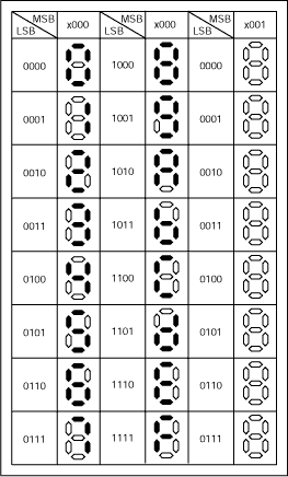
Figure 3. 7-segment display font
The MAX6954 has a built-in hexadecimal font for 7-segment displays, with 7 digits representing hexadecimal characters, and the 8th digit is used to select whether to light the decimal point (DP) (see Table 4). The data register has two levels, P0 and P1. Each display bit is represented by 2 bytes in the memory, one byte is located at P0 and the other is located at P1 (see Table 7). The data register is a mapped address mode, so each bit of data can be updated in P0 (registers 0x20 to 0x2F), P1 (registers 0x20 to 0x4 F), and can also be updated in two levels (registers 0x60 to 0x67). The data in the data register does not directly control the display of each segment in the 7-segment display. Instead, it is used to address the character generator that stores 7-segment font data (see Figure 3). The lower 7 bits of the register data (D6 to D0) are used to select characters from the font. The highest digit (D7) controls the decimal point (DP) display; set to 1 to display DP, and set to 0 to not display DP.
Table 4. Digital type data register format
| MODE | ADDRESS CODE (HEX) | REGISTER DATA | ||||||||
| D7 | D6 | D5 | D4 | D3 | D2 | D1 | D0 | |||
| 7-segment mode, writing digit data to use font map data with decimal place unlit | 0x20 to 0x2F 0x40 to 0x4F 0x60 to 0x6F | 0 | Bits D6 to D0 select font character | |||||||
| 7-segment mode, writing digit data to use font map data with decimal place lit | 0x20 to 0x2F 0x40 to 0x4F 0x60 to 0x6F | 1 | Bits D6 to D0 select font character | |||||||
If the flash function is disabled by the configuration register flash enable bit E (see Table 3), the data in the data register in P0 is used for display multiplexing. The data in the data register in P1 is not used. If the blinking function is enabled, the data multiplexing display in P0 and P1 is used alternately. The data in P0 and P1 are applied to different phases of the blinking clock alternately changing, thereby multiplexing the LED display to achieve the blinking function.
The following is an example of using MAX6954 driver to display Maxim / Dallas sales department telephone: 1 800 629 4642. Set the configuration register to disable the flashing function, so that you can control data bits 0 to 7 by writing data to registers 0x20 to 0x2F. Use the font diagram in Figure 3 to get the code corresponding to each character.
Table 5. Phone 800.629.4642 examples
| REGISTER ADDRESS (HEX) | DIGIT | CHARACTER | FONT MAP EQUIVALENT CODE | |
| DECIMAL | HEX | |||
| 0x20 | 0 | C | 0000 1100 | 0x0C |
| 0x28 | 0a | A | 0000 1001 | 0x0A |
| 0x21 | 1 | 1 | 0000 0001 | 0x01 |
| 0x29 | 1a | 1 | 0000 0001 | 0x01 |
| 0x23 | 3 | 8 | 0000 1000 | 0x08 |
| 0x2B | 3a | 0 | 0000 0000 | 0x00 |
| 0x24 | 4 | 0 | 1000 0000 | 0x80 |
| 0x2C | 4a | 6 | 0000 0110 | 0x06 |
| 0x25 | 5 | 2 | 0000 0010 | 0x02 |
| 0x2D | 5a | 9 | 1000 1001 | 0x89 |
| 0x26 | 6 | 4 | 0000 0100 | 0x04 |
| 0x2E | 6a | 6 | 0000 0110 | 0x06 |
| 0x27 | 7 | 4 | 0000 0100 | 0x04 |
| 0x2F | 7a | 2 | 0000 0010 | 0x02 |
Adjust the display brightness by writing data to register 0x02 (global brightness control register). The brightness can be adjusted between 0x00 (minimum brightness, 1/16 current) and 0xFF (maximum brightness, 15/16 current). You can also individually control the brightness of each bit. For more information on display brightness adjustment and other advanced features (such as GPIO and key scan), please refer to the MAX6954 data sheet.
Table 6. Routine command set
| REGISTER (HEX) | COMMAND (HEX) | FUNCTION |
| 0x07 | 0x01 | Enter display test mode |
| 0x07 | 0x00 | Exit display test mode |
| 0x04 | 0x01 | Exit shutdown mode, disable blinking and select global intensity control |
| 0x20 | 0x0C | Write "C" to digit 0 |
| 0x28 | 0x0A | Write "A" to digit 0a |
| 0x21 | 0x01 | Write "1" to digit 1 |
| 0x29 | 0x01 | Write "1" to digit 1a |
| 0x23 | 0x08 | Write "8" to digit 3 |
| 0x2B | 0x00 | Write "0" to digit 3a |
| 0x24 | 0x80 | Write "0." to digit 4 |
| 0x2C | 0x06 | Write "6" to digit 4a |
| 0x25 | 0x02 | Write "2" to digit 5 |
| 0x2D | 0x89 | Write "9." to digit 5a |
| 0x26 | 0x04 | Write "4" to digit 6 |
| 0x2E | 0x06 | Write "6" to digit 6a |
| 0x27 | 0x04 | Write "4" to digit 7 |
| 0x2F | 0x02 | Write "2" to digit 7a |
| 0x02 | 0xFF | Set global intensity to full-scale |
Table 7. MAX6954 / MAX6955 partial register address map
| REGISTER | ADDRESS (COMMAND BYTE) | ADDRESS (HEX CODE) | |||||||
| D15 | D14 | D13 | D12 | D11 | D10 | D9 | D8 | ||
| Decode Mode | R / active-low W | 0 | 0 | 0 | 0 | 0 | 0 | 1 | 0x01 |
| Global Intensity | R / active-low W | 0 | 0 | 0 | 0 | 0 | 1 | 0 | 0x02 |
| Scan Limit | R / active-low W | 0 | 0 | 0 | 0 | 0 | 1 | 1 | 0x03 |
| Configuration | R / active-low W | 0 | 0 | 0 | 0 | 1 | 0 | 0 | 0x04 |
| Display Test | R / active-low W | 0 | 0 | 0 | 0 | 1 | 1 | 1 | 0x07 |
| Digit Type | R / active-low W | 0 | 0 | 0 | 1 | 1 | 0 | 0 | 0x0C |
| Intensity 10 | R / active-low W | 0 | 0 | 1 | 0 | 0 | 0 | 0 | 0x10 |
| Intensity 32 | R / active-low W | 0 | 0 | 1 | 0 | 0 | 0 | 1 | 0x11 |
| Intensity 54 | R / active-low W | 0 | 0 | 1 | 0 | 0 | 1 | 0 | 0x12 |
| Intensity 76 | R / active-low W | 0 | 0 | 1 | 0 | 0 | 1 | 1 | 0x13 |
| Intensity 10a | R / active-low W | 0 | 0 | 1 | 0 | 1 | 0 | 0 | 0x14 |
| Intensity 32a | R / active-low W | 0 | 0 | 1 | 0 | 1 | 0 | 1 | 0x15 |
| Intensity 54a | R / active-low W | 0 | 0 | 1 | 0 | 1 | 1 | 0 | 0x16 |
| Intensity 76a | R / active-low W | 0 | 0 | 1 | 0 | 1 | 1 | 1 | 0x17 |
| Digit 0 Plane P0 | R / active-low W | 0 | 1 | 0 | 0 | 0 | 0 | 0 | 0x20 |
| Digit 1 Plane P0 | R / active-low W | 0 | 1 | 0 | 0 | 0 | 0 | 1 | 0x21 |
| Digit 2 Plane P0 | R / active-low W | 0 | 1 | 0 | 0 | 0 | 1 | 0 | 0x22 |
| Digit 3 Plane P0 | R / active-low W | 0 | 1 | 0 | 0 | 0 | 1 | 1 | 0x23 |
| Digit 4 Plane P0 | R / active-low W | 0 | 1 | 0 | 0 | 1 | 0 | 0 | 0x24 |
| Digit 5 ​​Plane P0 | R / active-low W | 0 | 1 | 0 | 0 | 1 | 0 | 1 | 0x25 |
| Digit 6 Plane P0 | R / active-low W | 0 | 1 | 0 | 0 | 1 | 1 | 0 | 0x26 |
| Digit 7 Plane P0 | R / active-low W | 0 | 1 | 0 | 0 | 1 | 1 | 1 | 0x27 |
| Digit 0a Plane P0 | R / active-low W | 0 | 1 | 0 | 1 | 0 | 0 | 0 | 0x28 |
| Digit 1a Plane P0 | R / active-low W | 0 | 1 | 0 | 1 | 0 | 0 | 1 | 0x29 |
| Digit 2a Plane P0 | R / active-low W | 0 | 1 | 0 | 1 | 0 | 1 | 0 | 0x2A |
| Digit 3a Plane P0 | R / active-low W | 0 | 1 | 0 | 1 | 0 | 1 | 1 | 0x2B |
| Digit 4a Plane P0 | R / active-low W | 0 | 1 | 0 | 1 | 1 | 0 | 0 | 0x2C |
| Digit 5a Plane P0 | R / active-low W | 0 | 1 | 0 | 1 | 1 | 0 | 1 | 0x2D |
| Digit 6a Plane P0 | R / active-low W | 0 | 1 | 0 | 1 | 1 | 1 | 0 | 0x2E |
| Digit 7a Plane P0 | R / active-low W | 0 | 1 | 0 | 1 | 1 | 1 | 1 | 0x2F |
| Digit 0 Plane P1 | R / active-low W | 1 | 0 | 0 | 0 | 0 | 0 | 0 | 0x40 |
| Digit 1 Plane P1 | R / active-low W | 1 | 0 | 0 | 0 | 0 | 0 | 1 | 0x41 |
| Digit 2 Plane P1 | R / active-low W | 1 | 0 | 0 | 0 | 0 | 1 | 0 | 0x42 |
| Digit 3 Plane P1 | R / active-low W | 1 | 0 | 0 | 0 | 0 | 1 | 1 | 0x43 |
| Digit 4 Plane P1 | R / active-low W | 1 | 0 | 0 | 0 | 1 | 0 | 0 | 0x44 |
| Digit 5 ​​Plane P1 | R / active-low W | 1 | 0 | 0 | 0 | 1 | 0 | 1 | 0x45 |
| Digit 6 Plane P1 | R / active-low W | 1 | 0 | 0 | 0 | 1 | 1 | 0 | 0x46 |
| Digit 7 Plane P1 | R / active-low W | 1 | 0 | 0 | 0 | 1 | 1 | 1 | 0x47 |
| Digit 0a Plane P1 | R / active-low W | 1 | 0 | 0 | 1 | 0 | 0 | 0 | 0x48 |
| Digit 1a Plane P1 | R / active-low W | 1 | 0 | 0 | 1 | 0 | 0 | 1 | 0x49 |
| Digit 2a Plane P1 | R / active-low W | 1 | 0 | 0 | 1 | 0 | 1 | 0 | 0x4A |
| Digit 3a Plane P1 | R / active-low W | 1 | 0 | 0 | 1 | 0 | 1 | 1 | 0x4B |
| Digit 4a Plane P1 | R / active-low W | 1 | 0 | 0 | 1 | 1 | 0 | 0 | 0x4C |
| Digit 5a Plane P1 | R / active-low W | 1 | 0 | 0 | 1 | 1 | 0 | 1 | 04D |
| Digit 6a Plane P1 | R / active-low W | 1 | 0 | 0 | 1 | 1 | 1 | 0 | 0x4E |
| Digit 7a Plane P1 | R / active-low W | 1 | 0 | 0 | 1 | 1 | 1 | 1 | 0x4F |
Analysis of advantages and disadvantages of 4G industrial routers
First, what is the classification of industrial routers?
Industrial Router (a communication device that can be divided into 2G routers, 2.5G routers, 3G routers and 4G routers according to network standards.
For users, you can communicate with the Internet by setting a default gateway on your PC or network device. In fact, the default gateway configured for network devices is the packet export for network devices. After the packet is sent to the Ethernet port of the router, the router performs the next job, so the router is an Internet relay.
Second, how do industrial routers work
So how does the router forward the packet? Just like getting somewhere, you need to place a route. This route is a routing table. This routing table contains all the destination network addresses owned by the router, as well as the best path to reach those networks through the router. This is because there is a routing table, so the router can forward packets according to the routing table. That's how routers work.
Understand what is an industrial router and how it works, it is not difficult to understand the advantages and disadvantages of the router. Here we focus on the advantages and disadvantages of 4G industrial routers.
Third, the advantages of 4G industrial routers
For networks interconnected via single-protocol industrial-grade wireless routers, the same or different protocols can be used at layers 1-2. Layer 3 uses the same routable protocol and requires the same or compatible protocols at layer 4 and beyond.
Industrial routers can perform complex routing calculations and are suitable for connecting three or more large networks with complex network topologies.
Industrial-grade routers can isolate broadcast storm information in the source network, thereby reducing and mitigating the impact of broadcast storms.
Multiprotocol industrial wireless routers can be used as network interconnection platforms using different communication protocols because they can connect to the network using different communication protocols.
The entire network router can also be used as a bridge to handle non-routable protocols.
Industrial 4G routers enable you to isolate unnecessary communications so that the interconnected network maintains its own area of independent management and control, thereby improving network security performance. Therefore, industrial-grade 4G routers are commonly used as firewalls to restrict access to the internal and external networks (Internet) of the LAN, as well as the internal areas of the LAN, and act as network masking.
It can provide reliable transport and prioritization services, and industrial LTE routers do not need to maintain a persistent connection between networks that communicate with each other.
Complete Netcom router network segmentation improves network performance and reduces host load.
Third, the advantages of 4G industrial routers
High price
When installing an industrial LTE router, it is difficult to install and maintain due to the large number of initial configurations
If you spend more time processing, the transmission performance of the entire network of the industrial router will decrease.
Unlike Bridges, routers across industrial networks are protocol-related. Each advanced protocol used for network connectivity must be configured separately, and an industrial-grade network-grade router with a separate protocol for each protocol must be provided.
Industrial Netcom routers do not support non-routed protocols, so when interconnecting multiple networks, there are restrictions on the protocols used by the connected networks.
4G Industrial Router,Sim Router Industrial,Industrial Lan Router,4G Modem Router Industrial
Shenzhen MovingComm Technology Co., Ltd. , https://www.movingcommiot.com