1 Introduction
The heat dissipation of a vehicle's system is an important indicator of its advancement, because each component and system of the vehicle has an optimal operating temperature range, and various performance indicators of parts and components can be guaranteed within this temperature range. At present, the development of China's vehicle system has entered the development stage of self-development and independent innovation. Due to the lack of actual vehicle test conditions and the complexity of the vehicle's working environment, the effective actual vehicle test data is seriously lacking and the test period is long. The reproducibility is poor, and it is impossible to provide accurate and effective actual vehicle test data to the engineering design department, which seriously affects the further development of the overall vehicle technology. Therefore, this article focuses on the development of a set of electronic circuits that can detect and record the dynamic parameters of the vehicle cooling system in real time using the single-chip control system, sensor technology, data storage technology, and real-time clock technology without changing the existing structure and performance of the vehicle. .
2 System overall architecture design
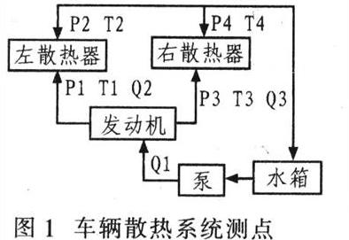
The heat dissipation system parameter test circuit is composed of the upper microcomputer and the lower single chip microcomputer control system. Figure 1 is a schematic diagram of the measurement points of the vehicle cooling system parameters. The main functions and technical indicators of the vehicle cooling system parameter test circuit are: (1) simultaneous detection of a total of 11 channels of data of temperature, pressure, and flow; (2) counting with a 10-bit A / D converter of the slave's leucorrhea Analog-to-digital conversion, to meet the requirements of system resolution, based on the concept of conversion before transmission to overcome the shortcomings of analog signals that are susceptible to interference in long-term transmission; (3) Use RS485 and USB serial bus transmission to achieve more Machine communication and communication with the host computer, and has the characteristics of fast transmission speed and strong anti-interference ability; (4) Use large-capacity data storage to meet the storage requirements of long-term large-capacity data.
3 Test system circuit design
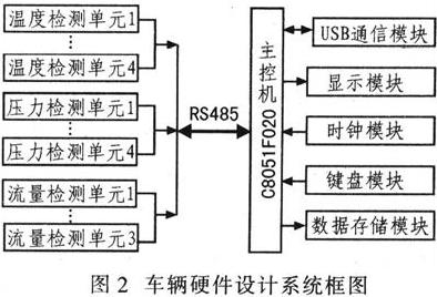
The system is mainly composed of data acquisition, liquid crystal display, keyboard, storage, RS-485 communication, USB communication and other circuits. Figure 2 is a block diagram of the system circuit design.
3.1 Circuit design of the main control unit
In the system circuit design, C8051F series single-chip microcomputer is used as the control device of the system. The single-chip microcomputer has a high-speed instruction execution speed. At the same time, it integrates complex peripheral functional components such as A / D conversion and crossbar switches into the single-chip microcomputer, which simplifies the circuit and improves the reliability of the system design.
The keyboard module enables the system to have manual independent control capabilities. The design of this module uses 4 & TImes; 4 non-array keyboard to realize the functions of confirmation, stop, clear, reset, communication, storage, time setting and so on. The row and column lines of the button are respectively connected to the P6 port of the MCU, and the “row scanning method†is used to determine which specific key on the keyboard is pressed. The display uses a dot matrix LCD module FM12864F, which is used to display the data of each channel, the current time, etc., in order to enhance the human-computer interaction effect. The serial clock DS1302 is used for clock design. In the circuit, we use P0, P0.5, P0.6, and P0.7 as the serial clock line, data line, and reset line of the clock device to connect Vcc2 to the backup power supply. In order to save time information in the case of power failure, this record is of great significance for the analysis of long-term continuous test system results and for finding the cause of abnormal data.
3.2 Design of data acquisition unit
The data collection unit collects the temperature, pressure and flow of the vehicle cooling system.
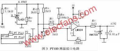
(1) Temperature signal collection uses platinum resistance PT100 to achieve temperature signal collection. The temperature measurement circuit is shown in Figure 3. R13, R14, VR2, and PT100 are used to form a measuring bridge. When the resistance value of PT100 and VR2 are not equal, the bridge outputs a millivolt-level differential pressure signal, which is amplified by LM324 and connected to the slave controller. The analog input channel AIN2 performs A / D conversion.
(2) Flow signal acquisition uses ultrasonic Doppler flowmeter to detect flow signal. In the measurement, the ultrasound transmitter is the same sound source. When the fixed frequency ultrasound emitted by the ultrasound transmitter is incident on these solid particles, there will be a difference between the ultrasound frequency reflected to the receiver and the transmission frequency. The frequency difference is the Doppler shift due to the movement of solid particles in the fluid. Since the amount of frequency shift is proportional to the fluid flow rate, measuring the frequency difference can obtain the flow rate and then the fluid flow rate.
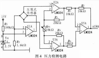
(3) The pressure signal is collected using a piezoresistive sensor to detect the pressure signal. The pressure measurement circuit is shown in Figure 4. In the system circuit design, VD1 uses LM385, whose stable voltage is 2.5 V, and provides a reference voltage of 1.5 mA constant current source for the sensor. U2 and U3 form a differential input and differential output amplifier circuit, which is converted into a single-ended signal output to ground through U5. The output signal is connected to the analog input channel AINO of C8051F012 for A / D conversion.
3. 3 peripheral circuit design
The peripheral circuit mainly cooperates with the controller to complete the vehicle cooling system parameter test, which is mainly composed of storage, RS485 communication, USB communication and other circuits.
3.3.1 Design of data storage circuit
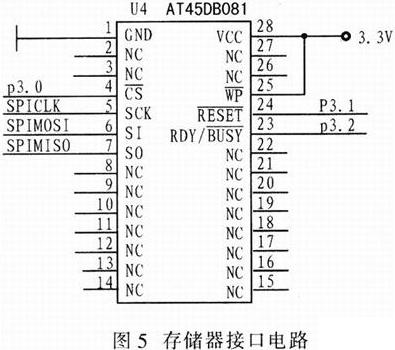
As can be seen from Figure 2, the temperature, pressure and flow parameters of the heat dissipation system need to be measured, a total of 11 channels. According to the design requirements, these 11 parameters are collected every 0.5 s and collected continuously for 2 h. If a 10-bit A / D converter is used, the required memory capacity is 309.375 K bytes. Therefore, AT45DB081 with a capacity of 8 Mbit is selected as a large-capacity memory, and the vehicle's operation data for a long period of time is stored as historical data. Figure 5 is the memory interface circuit. In the figure, the P0.2, P0.3 and P0.4 pins of C8051F020 are configured as the CLK, MISO and MOSI signal lines of the SPI through the crossbar, respectively, and the clock, serial output and The serial input pin is connected. Connect P3.0, P3.1 and P3.2 to the chip selection, reset and busy and idle pin states of AT45DB081 respectively.
3.3.2 Design of communication circuit
(1) RS-485 communication interface circuit In the test circuit, the master control machine sends commands, and the slave control machine receives commands and performs corresponding operations. Therefore, the RS-485 communication protocol is used to achieve multi-machine communication between the master and slave. The RS-485 standard interface is a differential drive structure. It converts the logic level to a potential difference through the transmission line driver to complete the signal transmission and improve the signal. Resistance to common mode interference. This system uses MAX485 driver for level conversion.
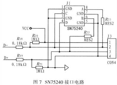
(2) USB communication interface circuit In the vehicle parameter test circuit, we extend the USB interface through PDIUSBD12 to realize the communication between the host computer and the host computer. In the system, PDIUSBD12 and C8051F020 adopt the connection mode of address data bus multiplexing. PDIUSBD12's ALE is used as an address latch signal, A0 is connected to a high level, and the address and data bus of C8051F020 are directly connected to the PDIUSBD12 data bus. The USB interface circuit is shown in Figure 6.

The vehicle's working environment is complex, and electromagnetic radiation is inevitable. Due to the limited ESD protection capability of PDIUSBD12, it is effective to prevent electrostatic discharge from damaging electronic components. In the system design, a transient voltage suppressor is connected in parallel between D-, D + and ground. Its SN75240 interface circuit is shown in Figure 7. When an instantaneous high-energy impact occurs at both ends of A, B or C, D, it can change the impedance value of both ends from a high resistance state to a low resistance state at a very high speed, absorbing a large current, thereby changing the The voltage is clamped to a small value to protect the circuit components behind from being damaged by the impact of transient high voltage.
3.3.3 Design of power circuit
At present, most of the vehicle's level voltage is 24 V, and when the parameter test device works normally, the power supply voltage required by the controller is 3 V, and the voltage required by other internal devices is 5 V. In order to ensure the normal operation of the parameter test device, the vehicle battery needs to convert the voltage to +3 V and +5 V to power the parameter test device.
4 Conclusion
The above hardware system, power system, communication unit and other peripheral circuits are made into printed circuit boards. Through testing, the circuit works well, and in the event of power failure and accidents, the dynamic data of the vehicle cooling system during the operation can be quickly and completely It is stored and the dynamic parameter value of the current channel is displayed on the display, which realizes the design requirements of the vehicle cooling system parameter test circuit.
best dc current sensor,best current sensor,ac current sensor,battery current sensor
Shanghai Zhilong Electronic Technology Co.,Ltd , https://www.zhilongsensor.com