Foreword: DCXO combined with MEMS and high-resolution phase-locked loop circuits, high-speed digital phase-locked loops that support minimum quantization noise design, and phase noise unaffected by frequency traction range, suitable for application to various RF and communication systems in.
Clock oscillator and RF system
As a reference signal source for frequency synthesis phase-locked loop, the clock oscillator is widely used in local oscillators, clock generation circuits and communication synchronization circuits of various RF systems (see Figure 1).
The local oscillator is multiplied by a phase-locked loop to generate the local oscillator drive signal required by the RF mixing circuit. The frequency accuracy and stability of the reference clock oscillator determine the accuracy and stability of the local oscillator signal and the RF transceiver operating frequency.
For RF systems with low frequency accuracy requirements, the built-in oscillator circuit of the RF chip and the external quartz crystal resonator form a reference clock oscillator, which can achieve a frequency accuracy of 10-4~10-5. RF communication systems requiring higher frequency error and environmental stability require a separate temperature compensated oscillator (TCXO) or a frequency-tunable traction temperature compensated oscillator (VC-TCXO) to achieve a 10-6~10-7 accuracy level. .
The constant temperature oscillator (OCXO) isolates the external temperature from the oscillator and enables the frequency accuracy to reach 10-8~10-9, meeting the time and frequency reference requirements of wireless base stations and high-capacity fiber-optic transmission network nodes.
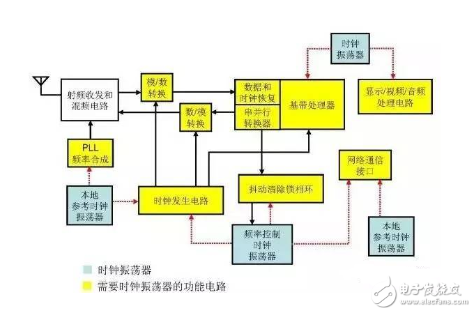
Figure 1: Application of Clock Oscillator in RF System
The clock generation circuit of the RF system provides a sampling clock for the digital to analog and analog to digital conversion circuits, a baseband digital signal processor clock, serial data, and a local clock for the clock recovery circuit. As a reference source for the clock generation circuit, the phase noise and jitter performance of the clock oscillator have a significant impact on the signal-to-noise ratio of the analog-to-digital signal conversion and the error rate of the data transmission and the jitter of the recovered clock.
Communication synchronization and jitter removal circuits for RF systems are also important applications for clock oscillators. Through wireless or wired signal transmission and clock recovery processes, the phase noise and jitter of the system clock increase due to channel noise. The jitter-clearing circuit uses a narrow-band phase-locked loop and a traction oscillator (VCXO) with low phase noise to filter the system clock phase noise for a low-jitter clock output.
The frequency stability and phase noise performance of all-silicon MEMS clock oscillators have made breakthroughs in recent years. MEMS oscillators also exhibit excellent environmental stability (full temperature, shock, vibration, electromagnetic interference, power supply noise) and device reliability.
Architecturally, the all-silicon MEMS clock oscillator combines a fixed-frequency MEMS resonator with a high-resolution, fractional-N phase-locked loop circuit that provides temperature compensation and frequency synthesis. Based on this architecture, various classes of clock oscillators have been developed—standard oscillators for single-ended and differential signal outputs, TCXO, VC-TCXO, VCXO, and digitally controlled oscillators (DCXO).
This article describes a comparison of MEMS-based DCXOs and traditional traction oscillators in jitter-clearing and communication genlock loop applications. An example is given to illustrate how to apply a high-performance DCXO and FPGA to design a simple, fully digital jitter-clearing phase-locked loop circuit.
Frequency control method
The oscillator can achieve frequency control by directly pulling the frequency or adjusting the frequency using a high-resolution phase-locked loop. The direct pull frequency of the VCXO adjusts the varactor voltage to change the resonant circuit capacitance, while the direct pull frequency DCXO switches the different resonant capacitors through the programmable switch.
The VCXO direct traction frequency adjustment using a quartz crystal resonator can maintain low phase noise, but the traction range is limited to approximately ±200 ppm. When system applications require a wider frequency pull range and low noise characteristics similar to crystal oscillators, users are more likely to choose phase-locked loop-based MEMS-controlled oscillator architectures because they can provide traction ranges up to ±1600ppm.
The phase-locked loop-based MEMS VCXO internal circuitry includes an analog-to-digital converter that converts the input voltage into a digital signal and drives a fractional-N phase-locked loop to regulate the output frequency. The architecture has better linearity in traction range and VCO gain (Kv) than direct traction.
The varactor-based VCXO has a VCO gain linearity of only 10%, while the phase-locked loop frequency pull can have a linearity of 0.1% to 1.0%. Good linearity simplifies the design of the phase-locked loop and is more stable over the entire operating range.
However, increasing the phase-locked loop VCXO pull range typically increases the phase noise of the oscillator output, which is one reason designers are reluctant to increase the traction range. DCXO can solve this problem. The DCXO can receive digitized frequency pull signals and directly drive the DCXO's fully digital phase-locked loop feedback divider and modulator without the need for an analog-to-digital converter, eliminating a source of near-carrier phase noise.
DCXO can achieve increased frequency pull range without increasing near-carrier phase noise and has a very linear gain response better than 1%, which is comparable to the best VCXO. The DCXO offers a number of programmable parameters so designers can have more choices of Kv, output frequency, and traction range parameters.
DCXO parameter selection
The absolute frequency draw range (APR) available for DCXO in real-world operating conditions is determined by the traction range, frequency stability, and long-term aging characteristics of the oscillator circuit.
For example, a ±150 ppm draw range, a frequency stability of ±10 ppm, and an aging characteristic of ±5 ppm of DCXO will have an APR of ±135 ppm. If the frequency stability level of the oscillator drops to ±50ppm, the available frequency range APR is also reduced to ±95ppm. Designers may need to consider the trade-off between required oscillator stability and device cost, while meeting system specifications.
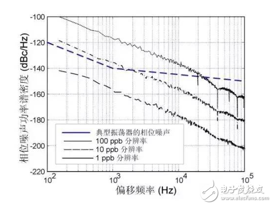
Figure 2: Phase noise due to frequency resolution quantization, DCXO 10 MHz output, frequency update rate 25,000 times per second
The digital phase-locked loop design using DCXO requires the selection of appropriate frequency resolution, frequency update rate, and update delay to minimize the quantization phase noise caused by frequency updates. By increasing the frequency update rate and frequency resolution, the quantization noise can be reduced below the oscillator's intrinsic phase noise level.
Figure 2 shows the 10MHz DCXO phase noise at different frequency resolution adjustments, with a frequency update rate of 25,000 times per second. The data in the figure shows that if the resolution of the DCXO frequency adjustment is higher than 10 ppb, the quantization noise introduced by the frequency update can be reduced to a level lower than the oscillator's intrinsic phase noise, so that the frequency adjustment does not affect the performance.
The frequency update rate is also a very important design parameter because the update rate is too low, causing the DCXO to accumulate large frequency phase errors over a relatively long period of time, resulting in larger frequency adjustment values ​​and increased quantization phase noise. However, for a DCXO that can be adjusted at 1 ppb resolution, even an update rate as low as 2,500 times per second is sufficient to ensure that the quantization noise does not affect the performance of the oscillator (see Figure 3).
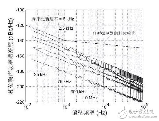
Figure 3: Effect of frequency update rate on near-carrier phase noise, DCXO frequency resolution 1 ppb
DCXO jitter clear circuit implementation
The DCXO applied to the jitter-clearing phase-locked loop should have a high enough frequency update rate, extremely high frequency resolution, low phase noise performance, and a frequency pull range suitable for the system. Figure 4 is a jitter-canceling circuit for a 125 MHz clock of an all-digital phase-locked loop based on DCXO and FPGA.
The SiT3907 DCXO is designed to provide up to 25,000 frequency update rates per second, high frequency resolution of 1 ppb, integrated phase jitter of less than 1 ps RMS (12 kHz to 20 MHz) and linear pull range of up to ±1600 ppm .
The all-digital phase-locked loop circuit includes an input clock divider, a phase accumulator, a loop filter, a loop state control circuit, an optional CIC filter, and a serial communication interface that drives the DCXO chip.
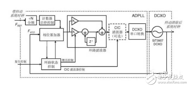
Figure 4: Block Diagram of Jitter Clear Circuit Based on DCXO and ADPLL
The phase accumulator is a start-stop counter that is driven by the feedback DCXO clock. The start and end of the counter period is triggered by the input clock divide pulse. The input clock prescaler value N determines the sample rate of the phase accumulator.
The loop filter needs to maintain a low bandwidth, typically no more than one tenth of the phase accumulator sampling rate. The loop state control circuit can reduce the loop gain after detecting the locked state, further improving the noise suppression capability.
The digital phase-locked loop circuit of Figure 4 also includes two additional functions to reduce phase noise and jitter. The first function is an update or reset signal of the loop state control circuit to minimize the accumulation of phase errors. The second function is an optional CIC filter that reduces the open loop gain. The open loop gain H(s) of the CIC filter is not turned on:
Where N is the ratio between the system clock and the phase comparator sampling frequency. The CIC filter mitigates the effect of gain variations on the output when the loop filter gain alternates between two values ​​during the lock process. In addition, adjusting the ratio between the gains Kp and Ki can increase stability and improve performance.
Experiments measure the effectiveness of phase noise, phase jitter, and jitter attenuation for this design. The measured data shows that the attenuation of the sinusoidal signal modulation jitter can be as high as 60 dB and results in a significant reduction in integrated phase jitter.
Figure 5 shows the effect of the jitter-canceling circuit on the clock signal; starting with a 125MHz system clock with significant jitter, reducing the wideband phase jitter from 157 ps RMS to 3.5 ps RMS yields a high performance for communication and networking applications Low jitter output clock.
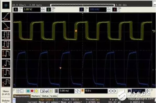
Figure 5: Comparing the 125 MHz system clock input with jitter (yellow, top) and the output clock after jitter clearing
Camping Light Tower,Outdoor Lighting Tower,Manual Type Light Tower,Balloon Metal Halide Light Tower
Wuxi Doton Power , https://www.dotonpower.com