How large is the market demand for 3D NAND, as evidenced by the fierce competition in this market!
May 29, 2018, citing South Korean media reports, Samsung plans to increase the current share of 64-layer 3D NAND products in 2018, and this year this year in the Hwaseong, Pyeongtaek factory to first mass production of 96-layer 3D NAND products, and even Plans to take the lead in the competition and start investing in the mass production of 128-layer 3D NAND.
Samsung's move may completely ignite the NAND Flash high-level stacking market in which “war†continues. The memory manufacturers in the United States, Japan, and South Korea will all participate in the war. The fierce competition in the market is even more difficult. Imagine.
"War" Continuous 3D NAND Flash
In the second half of 2017, 3D NAND manufacturers competed for mass production.
Samsung began mass production of 64-layer 3D NAND and used the new Pyeongtaek plant to increase production. Micron also promoted 64-layer 3D NAND smoothly. Toshiba and Western Digital began mass production of 64-layer 3D NAND from the second half of 2017.
At the same time, in order to reduce the cost of NAND Flash production and improve the competitiveness of its products, memory manufacturers in the United States, Japan, and South Korea have recently accelerated the development of higher-layer stacking and QLC four-bit cell storage products.
For example, Toshiba, the second largest manufacturer of NAND Flash in the world, announced in June 2017 with Western Digital that 96-layer 3D NAND using BiCS4 technology has been completed. Now, with the sales of Toshiba’s semiconductor business, it is widely believed that Toshiba will make rapid progress in NAND Flash in the future.
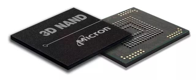
The NAND Flash products jointly developed by Micron and Intel also recently reported the successful development of 96-layer 3D NAND.
As for SK hynix, in July 2017, it began mass production of 72-layer (fourth-generation) 3D NAND flash memory chips. Although SK hynix currently ranks behind in the NAND Flash field, SK hynix also decided to complete 96-layer 3D NAND product development in 2018.
Will the number of 140-layer 3D NAND layers be far behind?
At the International Storage Seminar 2018 (IMW 2018) recently held, Applied Materials introduced the roadmap for the development of 3D NAND in the coming years. Among them, it is estimated that by 2020, 3D memory stacking can achieve 120 layers or even higher, reaching 140 layers in 2021, more than twice the current mainstream 64 layers.
At present, various manufacturers are making greater efforts in 3D NAND to increase the storage density of their own flash memory.
As mentioned earlier, Toshiba and Western Digital have plans to mass-produce new 96-layer BiCS4 memory chips this year. Samsung is also developing QLC NAND chips, which will achieve the 96-layer target in the fifth-generation NAND technology.
3D NAND technology is widely used nowadays. Its design is contrary to 2D NAND. The memory cells are not in one plane, but stacked one on top of the other. In this way, the storage capacity of each chip can be significantly increased. Instead of increasing the chip area or shrinking the cell, using 3D NAND can achieve larger structures and cell gaps, which is conducive to increasing the durability of the product.
However, 3D NAND technology also means that increasing the storage space requires constant increase in the number of stacked layers. The increase in the number of layers also means that the requirements for the process and materials will increase. In order to achieve a stack of 140 layers, new basic materials must be used.
Moreover, as the number of stacked layers increases, the height of the memory stack also increases. However, the thickness of each layer is shrinking. The previous 32/36-layer 3D NAND has a stack thickness of 2.5 μm, a layer thickness of approximately 70 nm, and 48 layers. The flash stack thickness is 3.5μm, the layer thickness is reduced to 62nm, the current 64/72 layer flash stack thickness is approximately 4.5μm, each layer thickness is reduced to 60nm, and to 140+ layers, the stack thickness will increase to approximately 8μm, each pair The stacked layers must be compressed to 45-50nm, and the stack thickness will be 1.8 times that of the original for each upgrade, and the layer thickness will be 0.86 times the original thickness.
With the continuous increase in the number of 3D NAND layers, the technical difficulty can be imagined!
QLC technology or will force
In fact, the way to reduce production costs per unit of capacity also includes improving data storage unit structure and controller technology.
At present, the structure types of memory cells are classified into the following types: SLC, MLC, TLC, and QLC.
SLC single-bit cells (each cell stores only 1 data), because of the stability, so the best performance, the longest life (the theory can be erased 10W times), the highest cost, is the earliest top particles.
MLC two-bit units (each cell stores 2 data), life (theory can be erased 1W times), the cost is balanced in several particles.
TLC three-bit unit (each cell stores 3 data), low cost, large capacity, but shorter life (the theory can be rewritable 1500 times), is currently the most mainstream product in flash memory.
QLC four-bit unit (each cell stores 4 data), lower cost, larger capacity, but shorter life (150 times the theory can be erased), want to become a successor to TLC products also need to solve many problems.
However, recently, Micron and Intel have taken the lead in adopting QLC technology to produce 3D NAND with a capacity of up to 1Tb and a stack of 64 layers. Currently, this product has been used for SSD shipments. Micron and Intel emphasized that this is the industry's first high-density QLC NAND. Flash.
Although Samsung has completed QLC technology research and development, Samsung may be based on strategic considerations. If it is too fast to commercialize it, the current product prices will probably be adjusted down. Plus, Samsung is the NAND Flash and SSD market leader, and there is no hurry to QLC. Reasons for commercialization. Toshiba said it plans to use QLC technology in 96-layer 3D NAND products.
In the future, if NAND Flash products use QLC technology that can store 4 four-bit units, it is expected to store about 33% more data than TLC technology. However, as the amount of stored data per storage unit increases, the life expectancy will also decrease. To improve the shortcomings in this area, memory vendors still need to overcome many problems!
Shenzhen Kate Technology Co., Ltd. , https://www.katevape.com