There are several different types and measurement methods for clock jitter, and the corresponding specifications, but most hardware designers don't have time to study this because the nuances of clock jitter specifications seem to be negligible for board designers. Trivial things. Designers tend to focus more on the most important design tasks, in order of priority. These are for FPGA logic, microprocessor complexes, data plane switch fabrics, control plane switch fabrics, RF signal links, power supplies, interconnects. Design tasks such as interworking problems, design simulation, and modeling.
Therefore, designers must assume that the reference clock jitter specifications from each chip vendor are related to the devices they are expected to use, and that these specifications have been fully and correctly determined.
But without some basic guidelines to follow, designers may specify excessive clock jitter requirements, resulting in more expensive clocking devices and increased unnecessary bill of materials (BOM). Or, in the worst case, the clock jitter requirement is reduced for a particular application, and the corresponding error may exceed the acceptable error rate level for a given application. This situation can only be discovered during the performance test of the original prototype board later in the product development cycle, and is therefore likely to affect the release time of the final product.
Most fundamental checkpoint
The first and most fundamental checkpoint that designers should consider is determining the most relevant type of clock jitter for a particular application. Table 1 summarizes some of the jitter classifications based on the type of application and the corresponding specification limits.
Table 1: Application-related jitter.
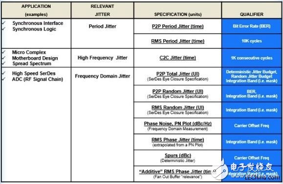
The period jitter is the most intuitive type of jitter. It simply refers to the deviation from the ideal (or average) of the period. It is the type of jitter associated with the synchronous interface and the logic design. The application examples include the microprocessor terminated with the synchronous memory. Interface, or synchronous state machine design inside the FPGA.
As the clock cycle is shortened or expanded, it can have a large impact on the setup time or hold time of the synchronous design, which is why cycle jitter is associated with these types of applications.
High frequency jitter, especially adjacent period (C2C) jitter, is the type of jitter associated with a spread spectrum clock. Spread-spectrum clocks intentionally induce low-frequency jitter to mitigate electromagnetic interference (EMI), which is traditionally a concern for consumer electronics. However, since spread spectrum is low frequency jitter, it does not affect adjacent period jitter measurements. For this reason, adjacent period jitter specifications can be used to quantify the jitter performance of a spread spectrum clock.
Carefully analyze frequency domain jitter
It is important to pay special attention to frequency domain jitter and its applicability in high speed serial communications. In particular, the reference clock jitter requirements for high-speed serializer/deserializer (SerDes) designs should be exhaustive. Frequency domain jitter is the least understood type of jitter and is therefore the most likely to cause some common board design flaws.
Figure 1 shows a phase noise (PN) curve generated by a spectrum analyzer that captures the spectral content of the clock signal and thus helps to understand the frequency characteristics of the clock jitter. This is also helpful in explaining the randomness of phase disturbances, which means random frequency perturbations, which in turn means random periodic perturbations.
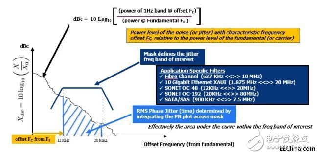
Figure 1: Phase noise (PN) curves are commonly used to represent clock jitter in the frequency domain.
Therefore, the PN curve represents random clock cycle jitter, but in the frequency domain. Mathematically, it is the strength of the clock signal's noise (ie, jitter) relative to the clock's fundamental frequency F0 at a particular fundamental frequency deviation.
The jitter strength at a particular frequency deviation can indicate how often the jitter value occurs, so a PN curve indicates how often a particular random frequency deviation occurs. The ratio of jitter strength to carrier is expressed in dBc/Hz. The lower the dBc/Hz value, the better, which means less jitter strength.
The root mean square (RMS) phase jitter is a jitter quantization value extrapolated from the PN curve that cannot be confused with the RMS period jitter of the time domain jitter specification. The converted RMS phase jitter value is largely an integral function whose value depends on the area of ​​the area under the PN curve.
But this area needs to be defined by an integration interval, or is often referred to as a "Mask." The Mask is associated with the transfer function of a particular application. The purpose is to limit or prevent the jitter quantization value from being within a range of frequencies, and the application's transfer function is no longer filtered. This means that any RMS phase jitter requirement must be defined by the range of integrations of interest.
A PN curve, along with the corresponding RMS phase jitter quantization value, is the type of clock jitter associated with the Serial/Deserializer (SerDes) application. Industrial clock standards such as Synchronous Digital Hierarchy (SDH), Synchronous Optical Network (SONET), Ethernet, PCI Express (PCIe), Serial RapidIO (SRIO), and SMPTE (American Society of Motion Picture and Television Engineers) use this type of clock jitter. Used to define the necessary reference clock jitter.
For reference, a representative SerDes communication channel is shown in Figure 2. The phase-locked loop (PLL) is a low-pass filter inherent to the input clock jitter, such that the transmitter (Tx) SerDes Clock Multiplier (CMU) PLL is used as a low-pass filter for reference clock jitter.
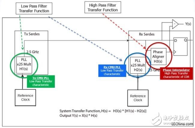
Figure 2: A representative high-speed serial communication channel.
The high frequency jitter of this clock is not transferred to the output of the PLL and therefore does not have any effect on the output jitter of the SerDes. The low pass filter characteristic of this Tx CMU phase locked loop determines the upper corner frequency of the integrated frequency band of interest.
In a similar manner, the receiver SerDes reference clock is multiplied by the internal receiver SerDes CMU phase-locked loop. This clock is then used in a phase interpolator based clock and data recovery (CDR) circuit, which acts as a high pass filter for reference clock jitter.
Therefore, the low frequency jitter of this clock is not passed to the phase aligner output for the CDR. The high pass filter characteristic of the receiver phase interpolator determines the lower corner corner frequency of the integrated band of interest.
All of these effects define the SerDes transfer function for a particular serial standard, as well as those that determine the frequency band or Mask of interest, such as the 1.875 MHz to 20 MHz band for 10G Ethernet.
Chip manufacturers' specifications are inconsistent
In addition to many different types of jitter and nuances, there are many uncertainties about how chip manufacturers can determine the required clock jitter for their devices. SerDes chip vendors determine the required reference clock jitter for their components, but device specifications such as physical layers, FPGAs, and processors are not necessarily consistent with the methodology and measurement details of industry serial interface standards.
For example, most network communication standards (such as Gigabit Ethernet, 10 Gigabit Ethernet, etc.) specify peak-to-peak (P2P) value total jitter as a percentage of a unit interval (UI), where a UI is at a given serial standard The equivalent of the time domain 1 bit interval. But the peak-to-peak total jitter UI is actually a SerDes eye closure specification to meet an acceptable bit error rate (BER), which is typically 10-12 according to the industry serial standard.
These standards do not define how much of the total jitter UI budget is allocated to the interconnect, optical, serial deserializer, or drive SerDes reference clock. As a result, board designers can only listen to chip vendors and the reference clock jitter specified in their data sheets. Often, these specifications are too conservative, giving most of the jitter budget to the integrated SerDes, leaving only a few for the reference clock that needs to drive SerDes.
To complicate matters, jitter specifications from clock chip vendors may be ambiguous and not necessarily complete. Some suppliers' descriptions of clock products are based on inappropriate specifications and measurement results, and are usually not suitable for the target application. There will be inconsistencies and lack of critical limits for a given specification.
Common jitter trap
For board designers, there are many pitfalls that can lead to errors. This section expands to discuss some of the more details of the common pitfalls listed below:
P2P random jitter specification is not qualified for target application BER
Apply clock jitter specifications and methodologies designed for communications applications to PCIe ports
The PN curve is generated to turn off the stray wave to meet the total phase jitter requirement (deterministic jitter is ignored by using random RMS phase jitter measurements)
The measurement/determination of jitter is only for the device, not the case configuration for a given application (eg w/built-in MultiSynth divider in integer mode)
Add RMS phase jitter measurement as a simple difference between input and output jitter, not the square root of the input and output jitter squared differences
For example, the Gaussian distribution skirt of the random period jitter shown in Figure 3 will extend indefinitely because the random jitter has no boundaries, so it is not realistic to actually measure the absolute maximum value of the P2P period jitter. However, jitter above one point in the Gaussian distribution can be given a probability. BER is specific to the application and is usually used for this purpose.
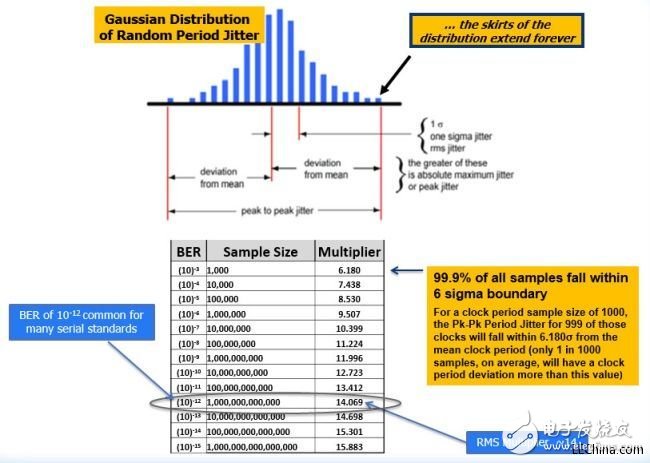
Figure 3: The Gaussian distribution of the random period jitter is infinitely extended.
There is no acceptable BER for the chip vendor, and the P2P cycle jitter specification is meaningless. However, this limitation is often difficult to see from the device's data sheet. For a given application, if an acceptable BER is known, the RMS period jitter for that given application can be calculated. So, it's important that designers have to know the correct BER for their application. Also, note that this method is not for periodic jitter because it can be used to calculate various types of RMS jitter. As an example, the calculation of an RMS phase jitter is as follows:
Consider the random phase jitter required by the 10GE PHY UI=0.18 UI
. . . Because the bit rate is 10.3125Gbps, 1 UI=96.9pS
. . . Assume that the acceptable BER for a given application is 10-12
Then, the required formula for calculating the corresponding RMS phase jitter is:
[(0.18)*(96.9pS)]÷(14.069) = 1.24pS
PCIe has become a common control plane interface for communication applications. Devices such as the Ethernet physical layer integrate PCIe ports for connecting out-of-band control plane microprocessors (micro). At least one well-known Ethernet PHY vendor has determined RMS phase jitter for their PCIe reference clocks in a manner similar to the way they determine RMS phase jitter for Ethernet ports in the same device, through the phase noise curve produced by the spectrum analyzer. Effectively extended. However, this method does not comply with the PCIe standard jitter method, as illustrated in Figure 4.
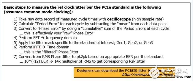
Figure 4: Seven steps to measure reference clock jitter for the PCIe standard.
The basic steps for measuring reference clock jitter according to the PCIe standard are as follows:
(assumed to be a common mode clock)
1) Use the oscilloscope (high sampling rate) to get the initial data record of the measured cycle time
2) Calculate the 'periodic error' for each cycle by subtracting the average from each data point
3) Converted to 'phase error' by cumulative summation of the period error of each cycle
... get your valid 'initial' phase error
4) Transition to the frequency domain by Fast Fourier Transform (FFT)
5) Apply a specific mask to the standard of interest, Gen1, Gen2, or Gen3
6) Perform an inverse fast Fourier transform (iFFT) operation and transform to the time domain
... get the 'filtered' phase error
7) Convert RMS phase jitter to peak-to-peak jitter based on appropriate standard bit error rate (BER) requirements
... 10-12 bit error rate, the corresponding peak to peak jitter is obtained by the RMS 14X multiplier
Instead, the PCIe method uses the original period samples measured by the oscilloscope and then applies the FFT, filter, and iFFT steps to derive the appropriate RMS phase jitter measurements. It is important to note that these two different methods can produce completely different results.
Therefore, designers may mistake the designed clock device for meeting or exceeding the PCIe reference clock jitter specification or standard, but these devices are not sufficient to drive the PCIe port because these PHY vendors have adopted different methods and/or filters. To determine the required reference clock jitter.
As previously discussed, P2P Total Jitter (UI) is a SerDes-specific data signal. This includes the contribution of deterministic and random jitter to the eye diagram of the data signal. It is widely believed that the deterministic jitter on the SerDes link is largely related to the link itself and other system barriers.
Random jitter is primarily attributable to the SerDes external reference clock and the PLL inside SerDes. But we know that the reference clock also has a certain amount of deterministic jitter. In addition, many PHY vendors' data sheets do not distinguish between random and deterministic jitter requirements that drive their SerDes reference clocks. For these reasons, another common design trap is to use the PN curve to quantify the total phase jitter of the clock device, including deterministic jitter, but the spurs are turned off (spurs are a shorthand for "periodic stray noise", Represents deterministic jitter of the clock). This deterministic jitter can be derived from the board design itself and/or the clock chip. Crosstalk, electromagnetic interference (EMI), switching power supply noise, and PLL fractional feedback dividers can all be sources of this deterministic jitter.
For the PN curve example shown in Figure 5, its special board design allows for significant spurious content to be measured at the PLL output. Unfortunately, these spurious noises are within the 12 kHz to 20 MHz integration range of interest for this application. Therefore, the total phase jitter of the reference clock has exceeded the specifications of the SerDes chip supplier, resulting in a higher BER. Using an EMI sniffer to analyze the root cause of these problems, it was discovered that this spur can be traced back to the synchronous buck switching regulator used to power the PLL, through board layout modifications and passive component changes. Can alleviate this problem.
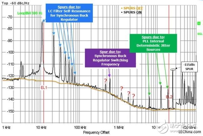
Figure 5: Example of a PN curve with spurious noise.
However, some of the spurious content comes from the PLL clock device itself. It is important to remember that any clock synthesizer can produce many unwanted sum and difference frequencies, and their strength may be large enough to appear significantly on the PN curve.
Today's excellent PLL designs use advanced silicon design techniques. These advances have helped to reduce the inherently generated random and deterministic (spur) jitter. However, for jitter-critical on-board clocks, designers need to verify that the corresponding phase jitter specification for a given clock device with a timer device is based on the PN curve obtained during spurious conduction.
A flow chart puts you on the right track
The flow chart shown in Figure 6 is intended to guide the board designer to the correct jitter specification for a specific application to properly select the clock chip.
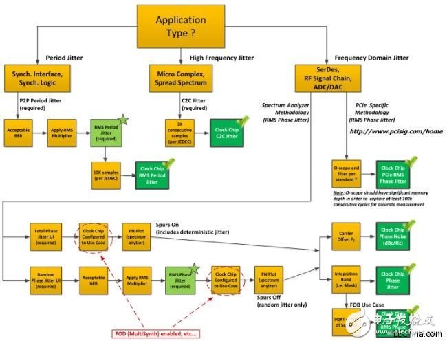
Figure 6: The flow chart helps determine the correct jitter for your application.
The first step is to determine the type of application. Is it a synchronous interface or synchronous logic design, a microprocessor reference clock specification or spread spectrum clock, a high speed serial communication or serial/deserializer design? In many board designs, all of these types of applications often require processing and they all have different jitter requirements.
For synchronous interfaces or synchronous logic designs, the involved jitter should be. Are you working from the P2P cycle jitter specification? If so, then you need to determine two key limitations: First, according to JEDEC (Joint Commission for Electronic Systems Engineering), the P2P cycle jitter you are using is based on a 10K sample size. Second, chip vendors provide you with a hypothetical BER for their specifications. With these two limits, a corresponding RMS period jitter specification can be derived to select the appropriate clock device.
If it is a consumer electronics application to achieve spread spectrum, then you may need to use adjacent cycle jitter specifications. According to the JEDEC standard, it is assumed that adjacent period jitter is measured across 1000 consecutive cycles. You need to confirm if this is the case, after which you will have a valid adjacent period jitter specification to determine the corresponding clock chip.
If it is a high-speed serial communication design, then you should first ask if the serial standard uses a traditional spread spectrum analyzer method to quantify phase noise. In addition, it is important to pay attention to what PHY vendors provide for the specification indicators, is the P2P total jitter UI, or the P2P random jitter UI?
It should be remembered that RMS is only for random jitter, and the random jitter requirement needs to be divided by the BER multiplier to get the corresponding RMS random jitter UI. For random jitter, you can use a PN curve that turns off the spurs to get the RMS phase jitter value by integration. However, if a spur PN curve is used to obtain deterministic jitter and then integrated in Mask, the corresponding value obtained is no longer RMS, but the total phase jitter.
The purpose of this flowchart is to guide you through a systematic approach to determining the correct jitter for your application. The process is designed to avoid the common board design pitfalls detailed in this article.
A useful clock device specification should be able to characterize the different output structures and the corresponding jitter capabilities of each structure. It can also provide specifications for the different jitter types described in this article, allowing designers to do their specific applications. limited. As an example, the universal frequency converter (UFT) shown in Fig. 7 can be considered.
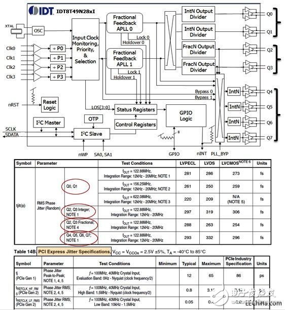
Figure 7: IDT8T49N28X Universal Frequency Converter.
This configurable clock device has several advanced features that are ideal for line-card applications. It delivers impressive high performance (such as low phase noise) and flexibility in a single device. To achieve this flexibility, the device uses a mix of integer and fraction based output dividers with RMS phase jitter values ​​for each output type, as detailed in this device specification. In addition, the device's data sheet highlights PCIe phase jitter performance in a separate table in accordance with the previously mentioned PCISIG methodology, noting the methodological differences in the serial interface standard.
It is important to realize that a configurable clock data table does not cover all application cases. Therefore, designers are encouraged to seek appropriate jitter performance for specific application cases, as the results may vary slightly.
Pure Green Color Led Display,0.56 Inch Grey Face Led Display,2 Digits Grey Face Led Display,0.56 Inch Led Display
Wuxi Ark Technology Electronic Co.,Ltd. , https://www.arkledcn.com