In the era of smart connectivity, data torrents are surging, and the demand for computing power is unprecedented. Intel continues to deliver ever-increasing computing power with leading-edge process technology and uses transistor density as the primary guideline for process development. Intel continues to break Moore's Law failure "magic" with breakthrough technology and continuous innovation. The main process innovations that have been widely used in the industry over the past 15 years have been driven by Intel and have always had at least three years of leadership.

Transistor density:
The primary criterion for measuring process leadership

At present, the name of the process node of some competitive merchant companies is not accurate, and it is impossible to correctly reflect where the process is located in the Moore's Law curve. Moore's Law means that the transistor density of each generation process is doubled. Throughout the history of development, the industry will reduce the process node by 30% compared with the previous generation. This linear scaling means that the transistor density is doubled, which is in accordance with Moore's Law. . Recently, perhaps because further process upgrades have become more and more difficult, some competing companies have deviated from Moore's Law, even though transistor density has increased little or not at all, they continue to promote the use of next-generation process node naming.
Transistor density is the primary criterion for measuring process leadership. Intel's proposed metric is based on the transistor density of standard cells, including the weighting factors that determine the typical design, resulting in a previously accepted transistor density formula:
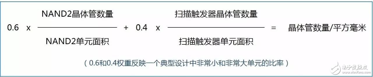
This formula can be used on any chip of any manufacturer and has been widely used in the industry to measure transistor density clearly and consistently, and to provide chip designers and customers with critical information to accurately compare processes from different manufacturers . By adopting this indicator, the industry can change the chaos of process node naming.
Intel 10 nm:
Transistor density is twice that of other competitive friends " 10 nanometers "
Intel's 10nm process uses third-generation FinFET technology, which is a full-generation generation compared to other competitive "10nm" processes. Intel's 10nm process has a transistor density of 198 million transistors per square millimeter, which is 2.7 times that of Intel's 14nm process, and is about twice that of other competitors in the industry.
Intel's 10nm process delivers up to 25% performance improvement and 45% power reduction compared to the previous 14nm process. The new enhanced 10nm process - 10++, can increase performance by 15% and reduce power consumption by another 30%.
Intel's 10nm process is scheduled to go into production by the end of 2017 and mass production in the first half of 2018.
Intel 14nm:
Transistor density is comparable to other competitive friends " 10 nanometers "
Compared to the 16/14 nm process of other competitors in the industry, Intel's 14nm process has a transistor density of about 1.3 times. The density of transistors in the "10nm" process of other competitors in the industry is comparable to that of Intel's 14nm process, but it is three years behind Intel's 14nm process.
Intel's 14nm process is in production with second-generation FinFET technology. Intel's 14nm process continues to optimize performance by up to 26% over the original 14nm process, and can reduce power consumption by more than 50% at the same performance. The performance of the Intel 14+ process is 12% higher than the original 14nm process, while the Intel 14++ process has improved performance by 24%, exceeding the industry's best 14/16nm process by 20%.
Ultra-shrinking technology:
Provides ultra-conventional transistor density
Ultra-shrink is a term used by Intel to describe a 2.7-fold increase in transistor density from 14 nm to 10 nm. Ultra-shrinking provides ultra-conventional transistor density for Intel's 14nm and 10nm processes and extends the process lifecycle. Although the development time between process nodes is more than two years, the super-compact makes it fully in line with Moore's Law.
22FFL
Internet of Things and mobile product innovation tools
22FFL is the world's first FinFET technology for low-power IoT and mobile products . It is based on Intel's 22nm/ 14nm process experience in recent years, bringing performance, power, density and ease of design. It will bring huge opportunities for innovation to China.
Compared to the previous 22GP (universal) process, the new 22FFL process can reduce leakage by up to 100 times. The 22FFL process provides comparable drive currents to 14nm process transistors while achieving higher area shrinkage than the industry's 28nm process.
Cutting-edge technology research and development: winning the future
Intel has a complete front-end R&D program, and some forward-looking projects under study include: Nanowire Transistor, III-V Materials, 3D Stacking, and Dense Memory. ), Scaling Interconnects, Extreme Ultraviolet Lithography, Spintronics, Neuromorphic Computing, and the like.
The electrolyte material inside the electrolytic capacitor, which has charge storage, is divided into positive and negative polarity, similar to the battery, and cannot be connected backwards.A metal substrate having an oxide film attached to a positive electrode and a negative electrode connected to an electrolyte (solid and non-solid) through a metal plate.
Nonpolar (dual polarity) electrolytic capacitor adopts double oxide film structure, similar to the two polar electrolytic capacitor after two connected to the cathode, the two electrodes of two metal plates respectively (both with oxide film), two groups of oxide film as the electrolyte in the middle.Polar electrolytic capacitors usually play the role of power filter, decoupling (like u), signal coupling, time constant setting and dc isolation in power circuit, medium frequency and low frequency circuit.Non-polar electrolytic capacitors are usually used in audio frequency divider circuit, television S correction circuit and starting circuit of single-phase motor.
Electrolytic Capacitor,Aluminum Electrolytic Capacitor,High Voltage Electrolytic Capacitor,12V Electronic Components Capacitor
YANGZHOU POSITIONING TECH CO., LTD. , https://www.cnpositioning.com