The article mainly introduces the semiconductor technology and CAD technology in the current RF integrated circuit research, and compares and discusses the respective characteristics of silicon devices and GaAs devices, RF integrated circuit CAD and traditional circuit CAD.
In recent years, the booming development of the wireless communication market, especially the rise of mobile phones and wireless Internet access services, has led to higher demands on wireless communication technologies. Small size, light weight, low power consumption and low cost are the development direction of wireless communication terminals, and radio frequency integrated circuit technology (RFIC) plays a key role. The emergence and development of RFICs have placed new demands on semiconductor devices, RF circuit analysis methods, and even receiver system architectures.
Semiconductor device technologyIn the RF field, performance and process requirements are much more complex than digital integrated circuits themselves. Among them, power consumption, speed, and yield are the most important parameters. At the same time, RF ICs also take into account noise (wideband and narrowband), linearity, gain, and power efficiency. In this way, optimized devices used in RF ICs have been continuously improved and developed. Different RF functional parts will be implemented on different semiconductor device processes. At present, the semiconductor processes used in RFIC are mainly Si, SiGe, GaAs and InP.
â— Silicon devices: silicon integrated circuits with silicon bipolar transistors (Si-Bipolar Transistors), silicon-complementary metal oxide semiconductors (Si-CMOS), silicon bipolar complementary metal oxide semiconductors (Bi-CMOS) or silicon Junction bipolar transistor (SiGe HBT).
At present, the communication frequency is mostly below 2 GHz. In addition to the power amplifier, the silicon integrated circuit is superior in the RF/IF module. The silicon process has a large amount of capacity, and can be composed of the RF/IF/MF to form a single-chip mixed mode integrated circuit. (single chip mixed mode IC), and can be operated from a single power supply. The price and integration are far more than the gallium arsenide devices, gallium arsenide and silicon integrated circuits. Because of different material properties, the design methods are also very different. Because silicon materials do not have a semi-insula TIon substrate, it is equivalent to circuit design on a high-loss substrate, and the gain of the device itself is low, to achieve high-frequency electrical properties comparable to gallium arsenide. Silicon RFICs are all based on transistor miniaturization (such as sub-micron RF CMOS) or material structure improvements (such as SiGe heterojunction transistors) to improve the device's characteristic frequency fT. It is also necessary to improve the isolation between the circuits and the Q value by means of trench isolation (trench isolaTIon). The process is complicated, the number of masks is numerous, the defect rate and cost are also greatly improved, and the high frequency model is also obvious due to the stray effect. grasp. At present, silicon technology is capable of RFICs above 5 GHz, but there are still insufficient RF front ends with low noise amplifiers, high power amplifiers and switches, so silicon process devices will be positioned in IF modules or low layers (low TIer). ) RF module.
It should be specially pointed out that in the wireless transceiver, the digital signal processing part uses a standard Si-CMOS process, which usually accounts for more than 75% of the chip area. The requirements of integration and power consumption make it impossible for him to use other than CMOS. Other processes are implemented, so only a CMOS integrated RF front-end can be implemented to achieve a monolithically integrated transceiver and ultimately a monolithically integrated mobile communication product. At present, with the development of CMOS technology, its unity gain cutoff frequency is close to the GaAs level, and some RF circuit front-end unit circuits and transceivers implemented by CMOS technology have appeared. This also makes it possible to implement single-chip integration of mobile communication products using a CMOS process. In addition, the CMOS process has higher integration, lower cost, and lower power consumption than other processes, making it the mainstream of RFIC development.
â— GaAs devices: GaAs devices have far higher electrical characteristics in high frequency, high power, high efficiency, and low noise index than silicon devices, depleted gallium arsenide field effect transistors (MESFETs) or high electron mobility transistors ( HEMT/PHEMT) can have 80% power added efficiency (PAE) under 3 V voltage operation, which is very suitable for long-distance and long communication time in high-level (high TIer) wireless communication. Both require a negative power supply, which will increase the cost of product use. The complicated long crystal and gate width control of HEMT devices also affect the consistency and productivity of the process. Enhancement mode E-mode MESFET/HEMT, because it does not require a negative power supply, while maintaining the excellent characteristics of its power amplifier, but its output power will be limited. Heterogeneous Bipolar Transistor (HBT) is another gallium arsenide device that does not require a negative power supply. Its power density, current drive capability, and linearity exceed FETs. High efficiency, high linearity microwave amplifier, HBT is the best choice for devices. HBT devices are superior in phase noise, high gm, high power density, breakdown voltage and linearity. In addition, it can operate from a single power supply, thus simplifying circuit design and sub-system implementation. It is very suitable for RF and IF transceiver modules. Developed, especially microwave signal sources and high linear amplifiers.
Circuit CAD technologyDesign methods and high-level computer-aided design tools are key to success in integrated circuit design. For the usual VLSI, there are a series of tools including synthesis, simulation, layout design, verification, test generation, etc. to support the entire design process. However, for RFIC, there is currently no complete set of CAD tools. The main front-end design tools are circuit-level simulation or simulation.
Insufficient SPICE simulation e#â— SPICE simulation deficiency
The usual circuit simulation uses an analog technology represented by SPICE, which supports multiple simulations. However, due to the characteristics of RFIC, there are many difficulties in using such circuit simulation techniques.
ZGAR Vape Pods 5.0
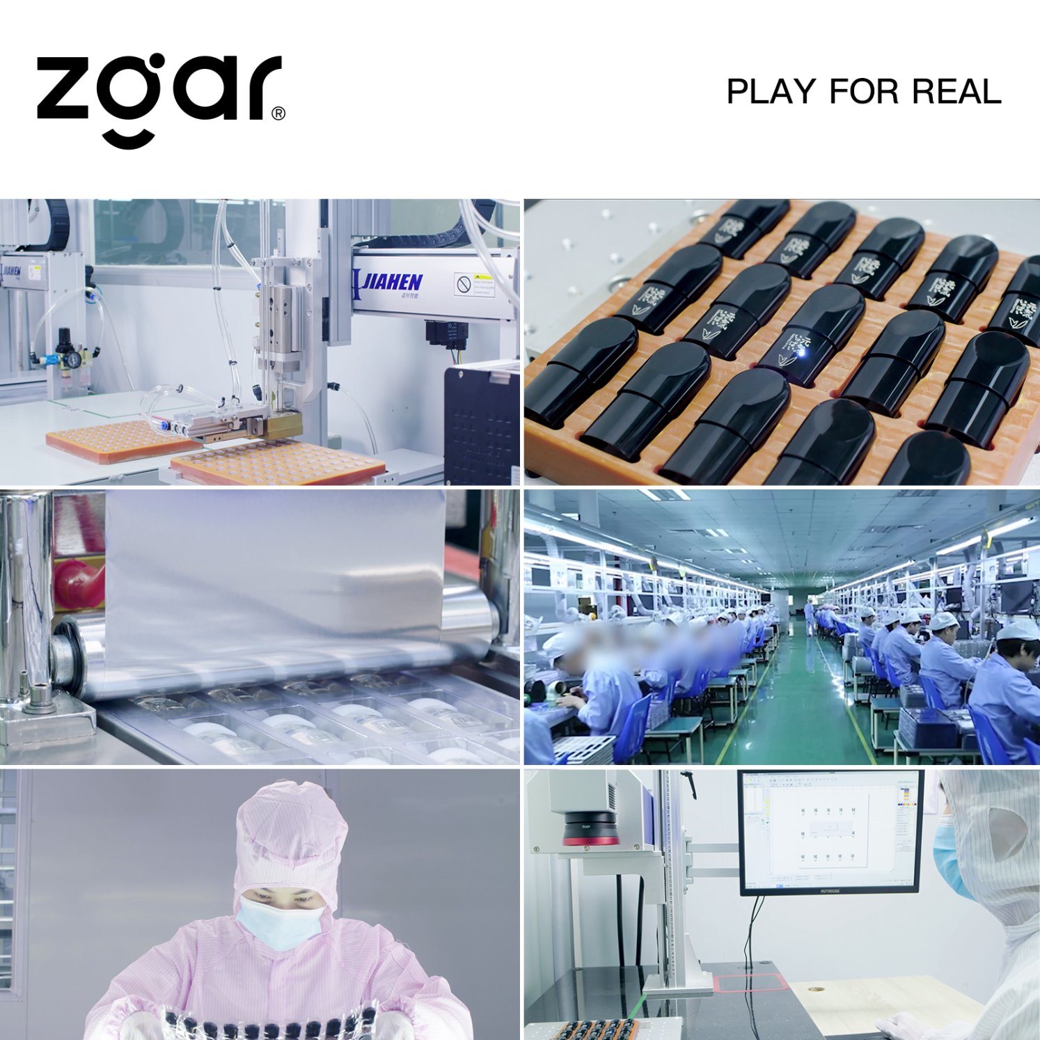
ZGAR electronic cigarette uses high-tech R&D, food grade disposable pod device and high-quality raw material. All package designs are Original IP. Our designer team is from Hong Kong. We have very high requirements for product quality, flavors taste and packaging design. The E-liquid is imported, materials are food grade, and assembly plant is medical-grade dust-free workshops.
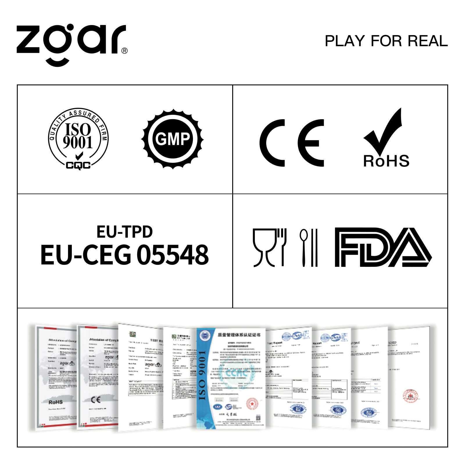
From production to packaging, the whole system of tracking, efficient and orderly process, achieving daily efficient output. WEIKA pays attention to the details of each process control. The first class dust-free production workshop has passed the GMP food and drug production standard certification, ensuring quality and safety. We choose the products with a traceability system, which can not only effectively track and trace all kinds of data, but also ensure good product quality.
We offer best price, high quality Pods, Pods Touch Screen, Empty Pod System, Pod Vape, Disposable Pod device, E-cigar, Vape Pods to all over the world.
Much Better Vaping Experience!


Pods, Vape Pods, Empty Pod System Vape,Disposable Pod Vape Systems
ZGAR INTERNATIONAL(HK)CO., LIMITED , https://www.oemvape-pen.com