World electronics have entered a packaging era that is faster, denser, thinner, less expensive, and requires more efficient heat dissipation. With the rapid commercialization of radio communication fields (such as mobile phones), there is a great pressure to reduce costs and improve performance. LTCC (Low Temperature Co-fired Ceramic) technology is a low-cost package solution with a short development cycle. This paper describes the feasibility of using LTCC technology to meet the requirements of the development of the microelectronics industry, especially high power RF circuits.
2LTCC Technology OverviewLTCC is a multilayer circuit made by laminating unsintered cast ceramic materials with printed interconnect conductors, components and circuitry and firing the structure into an integrated ceramic multilayer material. LTCC utilizes conventional thick film dielectric material casting instead of screen printing media slurry. The green tape is cut into a suitable size, and the alignment holes and the inner cavity are punched out, and the interconnecting through holes are formed by laser drilling or mechanical drilling. The conductor is screen printed or lithographically printed onto the various ceramic sheets along with the required resistors, capacitors and inductors. The layers of tiles were then aligned, laminated and co-fired at 850 °C. Assembly of substrates and surface mounting using existing thick film circuit production techniques.
3LTCC Process OverviewLTCC raw materials consist of a mixture of organic and inorganic ingredients. The organic component is a polymer binder and a plasticizer dissolved in the solution. Such as polyvinyl butyral, polyalloy aldehyde acetone and lower alkane (hydrocarbon) based acrylate copolymers. Acrylates are also used because they can be cleaned in air (or at temperatures between 300 ° C and 400 ° C under an inert atmosphere). It is required that the adhesive has a low Tg, high molecular strength, and good debinding characteristics. The adhesive is usually 5% by weight (the higher the percentage of the binder, the higher the shrinkage after firing).
The inorganic part consists of ceramic and glass, usually in a 1:3 ratio. The choice of ceramic depends on the characteristics required, such as coefficient of thermal expansion (CTE) and thermal conductivity. Preferred low CTE ceramics are quartz glass, mullite, cordierite and zirconia. In order to achieve a higher CTE, preferred ceramics are Al2O3, quartz, forsterite and calcium zirconate.
The choice of glass depends on the desired properties such as dielectric constant, adhesion, CTE and loss tangent. The glass softening point must be high enough to complete the debinding before the densification begins, as low as to ensure high density sintering. Commonly used plasticizers and solvents are dicarboxylic acid, acetone, xylene, methanol and ethanol. The components are then milled and homogenized in a paint-like suspension (called a glaze slurry), cast onto a moving carrier tape (usually a polyester film), and all solvent is removed through a drying zone. By controlling the blade gap, it is cast into the required thickness, viscosity and carrier tape shrinkage. The typical thickness tolerance for this process is ± 6%. Other casting techniques can be used to achieve smaller tolerances.
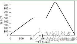
Figure 1 Typical burning curve of LTCC
The raw (unsintered) porcelain strip is then unrolled on a stainless steel table and cut into sheets (slightly larger than the size of the sheet). The ceramic chips were pretreated by heating at 120 ° C for about 30 minutes (or stored in an N2 drying oven for 24 hours). The pretreated green sheets are punched into the final working size using a punch press. Positioning graphics are also generated during this process.
The next step is to form through holes that are formed by mechanical stamping, drilling, or laser drilling techniques. The through holes are small holes (usually 5 mils to 8 mils in diameter) that are punched on the green sheets and used on different layers to interconnect the circuits. At this stage, the die holes are also punched to aid in the alignment of the laminations; the alignment holes are used for automatic video alignment when printing conductors and media.
This is followed by through-hole filling, which fills the vias with a specially formulated high solids content conductor paste using conventional thick film screen printing or extrusion. Programmable CNC punch presses are available for stainless steel or brass stencils. The shrinkage of the through-hole filler is matched to the shrinkage of the green tape.
The next step is to print and dry the conductor paste using standard thick film printing techniques. The via fill and conductor pattern were dried in a 120 ° C box oven for about 5 minutes. All resistors, capacitors and inductors are printed and dried at this stage as needed.
Followed by inspection, finishing and alignment. Inspect, organize, and align the different layers so that the alignment holes in each layer are concentric and ready to be laminated. During lamination (whether uniaxial or isostatic), the finished and aligned substrate layers are hot pressed together (typically 70 ° C, 10 minutes at 3000 psi). The laminate is then co-fired in one step. The area between 200 ° C and 500 ° C is called the organic debinding area (it is recommended to laminate the insulation for at least 60 minutes in this area). The laminate is then co-fired to a peak temperature (typically 850 ° C) for 5 minutes to 15 minutes. A typical debinding and firing curve for atmosphere firing metallization can take from 2 hours to 10 hours, as shown in Figure 1.
The fired parts are ready for a post-burning process, such as printing conductors and precision resistors on the top surface, and then firing in air. If Cu is used for metallization, sintering must be carried out in an N2 chain furnace. The circuit is then laser trimmed (if needed), tested, sliced, and inspected. Brazed leads or heat sinks are available in the LTCC package (if required). At this stage, the package is ready for the subsequent process as shown below.
1.ANTENK Insulation Displacement termination connectors are designed to quickly and effectively terminate Flat Cable in a wide variety of applications. The IDC termination style has migrated and been implemented into a wide range of connector styles because of its reliability and ease of use. Click on the appropriate sub section below depending on connector or application of choice.


SPECIFICATION
Current Rating: 1.0Amp
Insulation Resistance: 1000MΩ min
Contact Resistance: 20mΩ max
Withstand Voltage: 500V AC/DC
Operating Temperature: -40°C to +105°C
Contact Material: Phosphor Bronze
Contact Plating: Au Over Ni
Insulator Material: High Temperature plastic UL94V-0
Ribbon Cable Connectors,Cable Connector,Cable Assembly,Connector Flat Ribbon Cable,Box Header Connector,Latch Header Connector,IDC Socket Connector,Dip Plug Connector
ShenZhen Antenk Electronics Co,Ltd , https://www.antenkconn.com