Based on the ultra-low-power ARM Cortex-M0 processor core, the STM32F0 family integrates enhanced technologies and features for ultra-low-cost budget applications. This family of microcontrollers reduces the performance gap between devices using 8-bit and 16-bit microcontrollers and devices with 32-bit microcontrollers, enabling advanced and complex functions on cost-effective user terminal products. This article introduces the stm32 matrix keyboard schematic and program for everyone.
Stm32 matrix keyboard schematic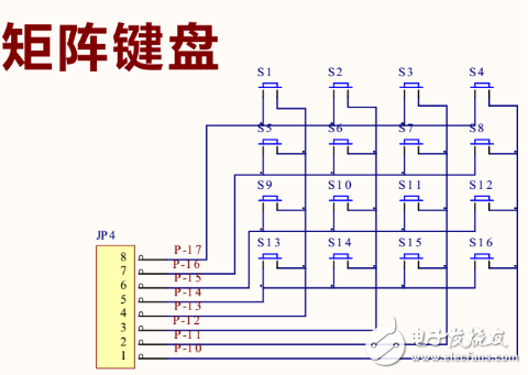
The main implementation: scan the matrix keyboard, send the detected data to the digital tube display through spi communication.
The main steps:
1: Initialize the clockVoid RCC_Configuration(void)
{
//----------Use external RC crystal-----------
RCC_DeInit (); / / initialized to the default value
RCC_HSEConfig(RCC_HSE_ON); //Enable external high speed clock
While(RCC_GetFlagStatus(RCC_FLAG_HSERDY) == RESET); //Wait for the external high-speed clock to be ready
FLASH_PrefetchBufferCmd(FLASH_PrefetchBuffer_Enable); //Enable Prefetch Buffer
FLASH_SetLatency(FLASH_Latency_2); //Flash 2 wait state
RCC_HCLKConfig(RCC_SYSCLK_Div1); //HCLK = SYSCLK
RCC_PCLK2Config(RCC_HCLK_Div1); //PCLK2 = HCLK
RCC_PCLK1Config(RCC_HCLK_Div2); //PCLK1 = HCLK/2
RCC_PLLConfig(RCC_PLLSource_HSE_Div1,RCC_PLLMul_9); //PLLCLK = 8MHZ * 9 =72MHZ
RCC_PLLCmd(ENABLE); //Enable PLLCLK
While(RCC_GetFlagStatus(RCC_FLAG_PLLRDY) == RESET); //Wait till PLLCLK is ready
RCC_SYSCLKConfig(RCC_SYSCLKSource_PLLCLK); //Select PLL as system clock
While(RCC_GetSYSCLKSource()!=0x08); //Wait till PLL is used as system clock source
}
2: Configuration pinVoid GPIO_Configuration(void)
{
GPIO_InitTypeDef GPIO_InitStructure;
SPI_InitTypeDef SPI_InitStructure;
RCC_APB2PeriphClockCmd (RCC_APB2Periph_GPIOD, ENABLE); / / turn on the GPIOD peripheral clock
GPIO_InitStructure.GPIO_Pin = GPIO_Pin_0|GPIO_Pin_1|GPIO_Pin_2|GPIO_Pin_3;//D0~D3
GPIO_InitStructure.GPIO_Speed ​​= GPIO_Speed_50MHz;
GPIO_InitStructure.GPIO_Mode = GPIO_Mode_IPU; / / pull-up input
GPIO_Init(GPIOD, &GPIO_InitStructure);
GPIO_InitStructure.GPIO_Pin = GPIO_Pin_4|GPIO_Pin_5|GPIO_Pin_6|GPIO_Pin_7;//D4~D7
GPIO_InitStructure.GPIO_Speed ​​= GPIO_Speed_50MHz;
GPIO_InitStructure.GPIO_Mode = GPIO_Mode_Out_PP; / / push-pull output
GPIO_Init(GPIOD, &GPIO_InitStructure);
/ / Initialize the pin level
GPIO_SetBits(GPIOD, GPIO_Pin_0 | GPIO_Pin_1| GPIO_Pin_2| GPIO_Pin_3);
GPIO_ResetBits(GPIOD, GPIO_Pin_4 | GPIO_Pin_5| GPIO_Pin_6| GPIO_Pin_7);
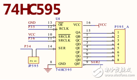
RCC_APB2PeriphClockCmd(RCC_APB2Periph_GPIOA |RCC_APB2Periph_SPI1, ENABLE); //Enable SPI1 and GPIOA peripheral clocks
GPIO_InitStructure.GPIO_Pin = GPIO_Pin_4|GPIO_Pin_5|GPIO_Pin_6|GPIO_Pin_7;//Set the four pin modes of SPI
GPIO_InitStructure.GPIO_Speed ​​= GPIO_Speed_50MHz;
GPIO_InitStructure.GPIO_Mode = GPIO_Mode_AF_PP; //Multiple push-pull output
GPIO_Init(GPIOA, &GPIO_InitStructure);
GPIO_InitStructure.GPIO_Pin = GPIO_Pin_1; //Set GPIO A1 pin for latching 74HC595 output
GPIO_InitStructure.GPIO_Speed ​​= GPIO_Speed_50MHz;
GPIO_InitStructure.GPIO_Mode = GPIO_Mode_Out_PP; / / push-pull output
GPIO_Init(GPIOA, &GPIO_InitStructure);
SPI_InitStructure.SPI_Direction = SPI_Direction_2Lines_FullDuplex; // SPI data mode two-wire bidirectional full duplex
SPI_InitStructure.SPI_Mode = SPI_Mode_Master; //SPI mode main mode
SPI_InitStructure.SPI_DataSize = SPI_DataSize_8b; //Set the SPI data size
SPI_InitStructure.SPI_CPOL = SPI_CPOL_High; //Set the polarity of the clock
SPI_InitStructure.SPI_CPHA = SPI_CPHA_2Edge; //Set the phase of the clock
SPI_InitStructure.SPI_NSS = SPI_NSS_Hard; //NSS pin hardware set
SPI_InitStructure.SPI_BaudRatePrescaler = SPI_BaudRatePrescaler_64; / / prescaler value
SPI_InitStructure.SPI_FirstBit = SPI_FirstBit_MSB;// Data is transferred from high bits
SPI_InitStructure.SPI_CRCPolynomial = 7; //CRC value
SPI_I2S_DeInit(SPI1); //Reset the peripheral SPI1 register to the default value;
SPI_Init(SPI1, &SPI_InitStructure);
SPI_Cmd (SPI1, ENABLE); / / enable SPI1 peripherals
}
3: Write matrix keyboard scan function KEY.c
U8 shu=16;
Void KeyScan(void)
{
U8 i;
If((GPIO_ReadInputData(GPIOD) & 0x0f) != 0x0f )
{
Delay_MS(20);
If((GPIO_ReadInputData(GPIOD) & 0x0f) != 0x0f )
{
GPIO_SetBits(GPIOD, GPIO_Pin_4 | GPIO_Pin_5| GPIO_Pin_6);
GPIO_ResetBits(GPIOD, GPIO_Pin_7);
Switch(GPIO_ReadInputData(GPIOD) & 0x0f)
{
Case 0x07: shu=0; break;
Case 0x0b: shu=1; break;
Case 0x0d: shu=2; break;
Case 0x0e: shu=3; break;
}
GPIO_SetBits(GPIOD, GPIO_Pin_4 | GPIO_Pin_5| GPIO_Pin_7);
GPIO_ResetBits(GPIOD, GPIO_Pin_6);
Switch(GPIO_ReadInputData(GPIOD) & 0x0f)
{
Case 0x07: shu=4; break;
Case 0x0b: shu=5; break;
Case 0x0d: shu=6; break;
Case 0x0e: shu=7; break;
}
GPIO_SetBits(GPIOD, GPIO_Pin_4 | GPIO_Pin_6| GPIO_Pin_7);
GPIO_ResetBits(GPIOD, GPIO_Pin_5);
Switch(GPIO_ReadInputData(GPIOD) & 0x0f)
{
Case 0x07: shu=8; break;
Case 0x0b: shu=9; break;
Case 0x0d: shu=10; break;
Case 0x0e: shu=11; break;
}
GPIO_SetBits(GPIOD, GPIO_Pin_7 | GPIO_Pin_5| GPIO_Pin_6);
GPIO_ResetBits(GPIOD, GPIO_Pin_4);
Switch(GPIO_ReadInputData(GPIOD) & 0x0f)
{
Case 0x07: shu=12; break;
Case 0x0b: shu=13; break;
Case 0x0d: shu=14; break;
Case 0x0e: shu=15; break;
}
GPIO_SetBits(GPIOD, GPIO_Pin_0 | GPIO_Pin_1| GPIO_Pin_2| GPIO_Pin_3);
GPIO_ResetBits(GPIOD, GPIO_Pin_4 | GPIO_Pin_5| GPIO_Pin_6| GPIO_Pin_7);
While((i"50)&&((GPIO_ReadInputData(GPIOD) & 0x0f) != 0x0f))
{
i++;
Delay_MS(10);
}
}
}
}
Void Display_Data(u8 data)
{
U8 i=data;
PAOut(1)=0;
SPI_I2S_SendData(SPI1,DSY_CODE[i]);
Delay_MS(2);
PAOut(1)=1;
Delay_MS(1000);
}
5: main function#include"stm32f10x_lib.h"
#include
#include"Exboard.h"
U8 DSY_CODE[]={0xc0,0xf9,0xa4,0xb0,0x99,0x92,0x82,0xf8,0x80,0x90,0x88,0x83,0xc6,0xa1,0x86,0x8e,0xff};
Int main(void)
{ //u8 i;
RCC_Configuration();
GPIO_Configuration();
//EXTI_Configuration();
//NVIC_Configuration();
While(1)
{
KeyScan();
Display_Data(shu);
}
}
Appendix: Exboard.h#ifndef _EXBOARD_H
#define _EXBOARD_H
#endif
#include"stm32f10x_lib.h"
#define GPIOA_IDR (GPIOA_BASE+0x08)
#define GPIOA_ODR (GPIOA_BASE+0x0c)
#define GPIOB_IDR (GPIOB_BASE+0x08)
#define GPIOB_ODR (GPIOB_BASE+0x0c)
#define GPIOC_IDR (GPIOC_BASE+0x08)
#define GPIOC_ODR (GPIOC_BASE+0x0c)
#define GPIOD_IDR (GPIOD_BASE+0x08)
#define GPIOD_ODR (GPIOD_BASE+0x0c)
#define GPIOE_IDR (GPIOE_BASE+0x08)
#define GPIOE_ODR (GPIOE_BASE+0x0c)
#define GPIOF_IDR (GPIOF_BASE+0x08)
#define GPIOF_ODR (GPIOF_BASE+0x0c)
#define GPIOG_IDR (GPIOG_BASE+0x08)
#define GPIOG_ODR (GPIOG_BASE+0x0c)
#define BitBang(Addr,BitNum) *((volatile unsigned long*)(((Addr&0xf0000000)+ 0x2000000)+(((Addr&0xfffff)""5)+(BitNum"(2))))
#define PAIn(n) BitBang(GPIOA_IDR,n)
#define PAOut(n) BitBang(GPIOA_ODR,n)
#define PBIn(n) BitBang(GPIOB_IDR,n)
#define PBOut(n) BitBang(GPIOB_ODR,n)
#define PCIn(n) BitBang(GPIOC_IDR,n)
#define PCOut(n) BitBang(GPIOC_ODR,n)
#define PDIn(n) BitBang(GPIOD_IDR,n)
#define PDOut(n) BitBang(GPIOD_ODR,n)
#define PEIn(n) BitBang(GPIOE_IDR,n)
#define PEOut(n) BitBang(GPIOE_ODR,n)
#define PFIn(n) BitBang(GPIOF_IDR,n)
#define PFOut(n) BitBang(GPIOF_ODR,n)
#define PGIn(n) BitBang(GPIOG_IDR,n)
#define PGOut(n) BitBang(GPIOG_ODR,n)
#define KEY1 PEIn(0)
#define LED1 PDOut(13)
#define KEY2 PCIn(13)
#define LED2 PGOut(14)
Void Delay_MS(u16 dly);
/
Void RCC_Configuration(void);
Void GPIO_Configuration(void);
//void EXTI_Configuration(void);
//void NVIC_Configuration(void);
Extern void KeyScan(void);
Void Display_Data(u8 data);
Extern u8 shu;
Fiber Optic Patch Panel,Fiber Patch Panel,Fiber Distribution Panel,Optical Patch Panel
Cixi Dani Plastic Products Co.,Ltd , https://www.danifiberoptic.com