Manufacturing documents for flexible circuit boards or hard and soft boards
In the last issue of the blog on hard and soft printed circuit boards, I talked about the typical process flow for manufacturers of flexible boards. Understanding the manufacturing process is very important for designing a hard-flex board or a flexible circuit board. At the same time, it also tells you the data provided by the successful manufacturing of the design board. If you haven't read Part 1 and Part 2 of this series of blogs yet, read it here and here, and then continue.
Manufacturing documentsLet's talk about manufacturing documents. They are very important. We use manufacturing documents to tell producers what we want, but they are also important factors that cause misunderstandings or mistakes that result in costly delays. Fortunately, we can refer to a number of criteria to ensure that we can communicate with the manufacturer, especially IPC-2223B (my blog also refers to this standard).
This can be attributed to the following golden rules:
Make sure your manufacturer has the ability to make your design's hard and soft boards.
Make sure that they work with you from the time they build the cascading structure so that the design can meet their production process.
Use IPC-2223 as a design reference and ensure that manufacturers use the same or related IPC standards so that you use the same terminology as they do.
As soon as possible let them participate in the design process.
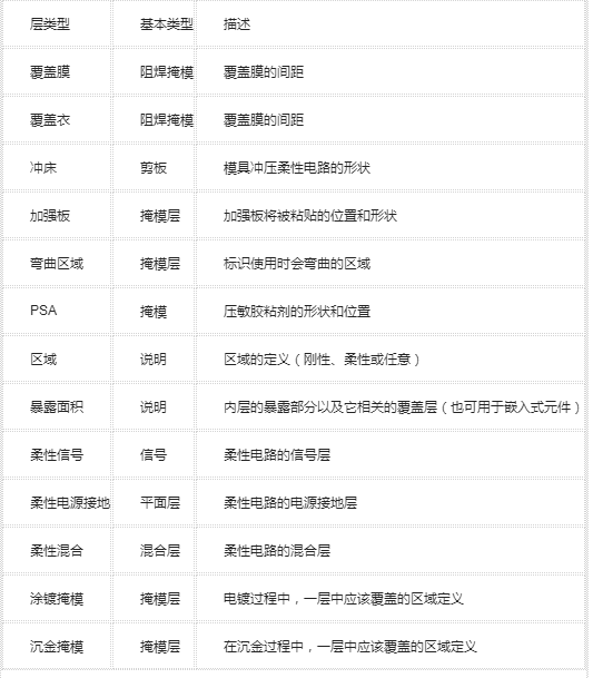
Output data setAfter visiting some local board makers who were able to make hardware and software boards, we found that many designers still sent gerber files to their board makers. However, the preferred choice should be ODB++ v7.0 or higher because of the addition of specific layer types in its work matrix that allow GenFlex ® and similar CAM tools to clearly identify them. As shown in Table 1, contains a subset of data.
Table 1: Sub-set of ODB++ Layer Types for GenFlex (V7.0 and later)
(Source: ODB++ V7.0 specifications)
If we use Gerber or an earlier version of ODB++, we will have a lot of trouble. That is, manufacturers need to separate the shear path and die-cut pattern from the rigid and flexible circuit sections. In fact, we need to use mechanical layer film to show the avoidance requirements on rigid boards, and what parts of the flexible circuit area will be exposed; show how to use overlays to reinforce the pads of components mounted on flexible circuits.
In addition, special attention needs to be paid to the pair of drilled holes and the plated through hole, because the drilling from the rigid plate to the opposite side of the flexible plate requires a double drilling, which increases the cost and reduces the yield.
The real question as a designer is, how do you define these areas, layers, and stacks?
Use a table to define a stacked stackThe most important document available to manufacturers is undoubtedly the stacked stack. In order to make a hard-soft board, it is also necessary to provide different stacks in different fields and to clearly identify them. A simple method is to duplicate the outline of the board on the mechanical layer, and identify the areas where different stacked stacks exist, and put the corresponding stack structure table next to it. Figure 1 below is an example.
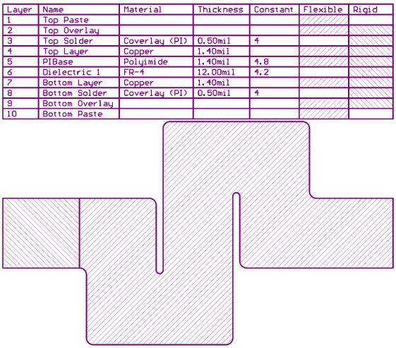
Figure 1: The stack diagram shows the fill patterns of the hard and soft circuit areas.
In this example, I used a different fill pattern matching the stack area to indicate which stacks were included in the flex or rigid sections. It can be seen here that "insulation 1" uses FR-4 because it is a stiffener.
This creates new problems. We also need a 2D space to define where it is curved or folded, where components and other important objects can cross the boundary between rigidity and flexibility. I will elaborate on this later.
Passing PCB design intentWe all know that pictures are worth a thousand words. If you can generate a 3D image showing the areas of flexibility and rigidity, this will help manufacturers to better understand our intentions. Many people are currently using MCAD software to achieve this view, they import the PCB design of the STEP file into the MCAD software. Figure 2 is an example of a reference to this concept.
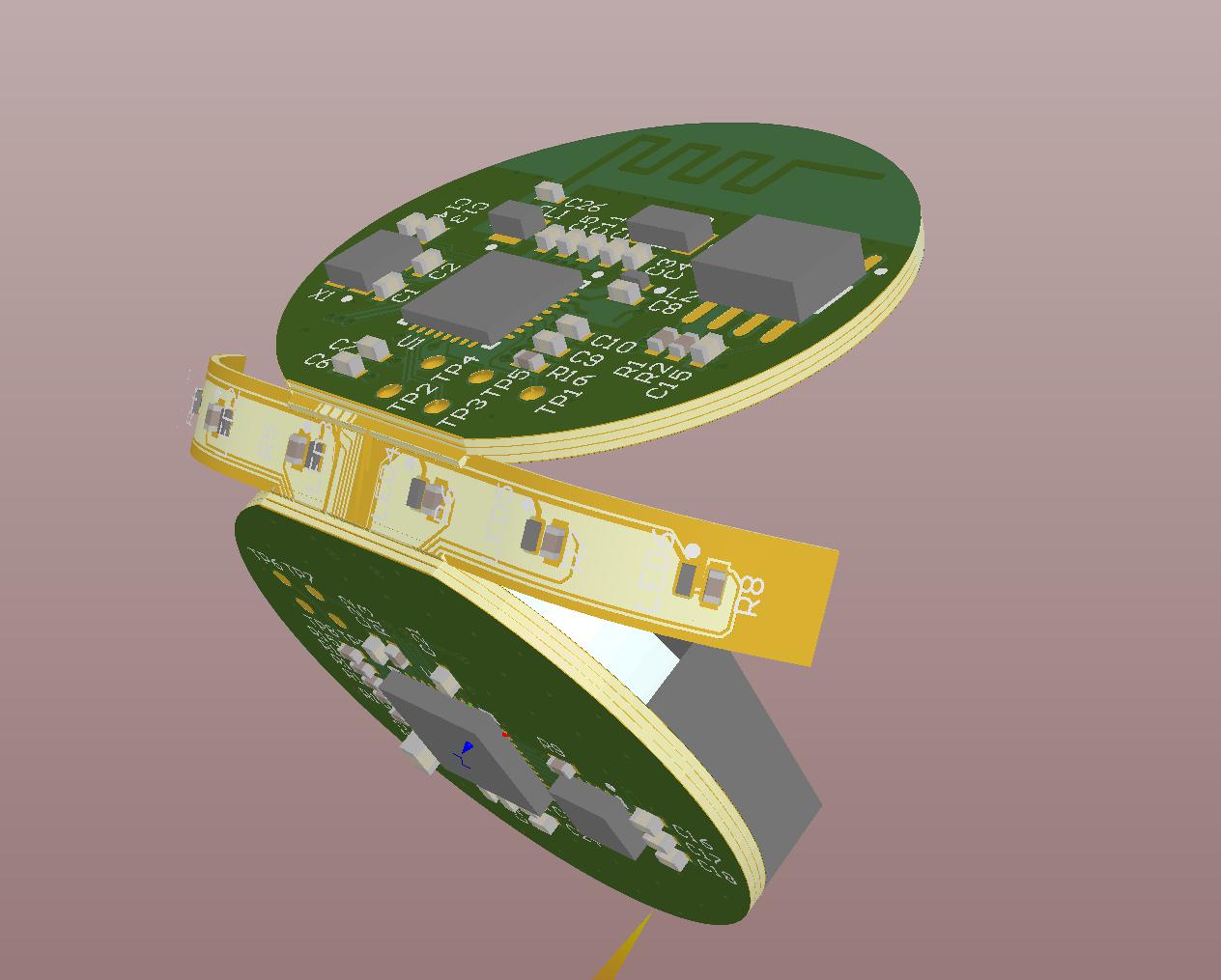
Figure 2: Bending mechanics model showing design intent.
Another advantage is that it can help us to check the mutual interference between the flexible board and the flexible board and the flexible board and the rigid board to avoid a huge mistake.
Component placementAs you can see from the figure above, a hard and soft board means that components can be placed in the middle layer, not just the top and bottom layers. This is a bit tricky in PCB design software because the components must usually be placed at the top and bottom layers. Therefore, we need the ability to place components in the middle layer.
Fortunately, AlTium Designer can place pads on any layer, so this is possible. In addition, silk screens can be printed on flexible circuits. This is not a problem because the cover material can be well adhered to the screen printing ink. The key is to select enough contrasting ink colors through the overlay material. The definition of silk screens can be somewhat affected because it passes through the cover film and the fine spacing between them. Again, it is necessary to negotiate with the manufacturers to find feasible and economical practices.
Comment: If we plan a certain area on the PCB board for connecting flexible boards and place components on these areas, this is a reasonable area for placing embedded components. We need to generate a very clear set of documents that show the location and lamination of the cuts. This can cause limitations due to manufacturing methods, such as double drills or multiple presses. Therefore, it is very important to accurately convey your intentions and minimize individual openings. It is best to avoid crossing the board on both sides.
Comment: Define Flex Cuts
Please note that in Figure 1, why is there no right angle bend, but what is the minimum radius of each corner? The IPC recommends a radius greater than 1.5mm (approximately 60 mils), which greatly reduces the possibility of tearing the flexible circuit at the corners. For the same reason, holes with a diameter of 3 mm (1â„8) or more to prevent tearing are placed at both ends of the groove and slit in the flexible circuit. See the demonstration of the following example.
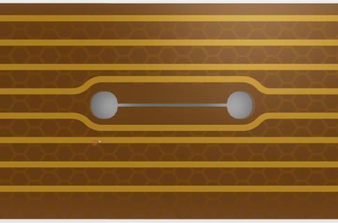
Figure 3: Grooves, slits, and interior corners should have arcs with a minimum radius of 1.5 mm between the tear-proof or tangential lines.
In order to produce a reliable hard and soft bonded board product, there are many considerations for the end user of the manufacturer and the flexible circuit, including the design considerations for the copper skin pattern. In the next blog, I will discuss what these should and should not do. Stay tuned!
The main wiring material in the network integrated wiring system is the Network Cable, including twisted-pair cable, optical fiber, optical fiber and so on.In order to protect the wiring line, ensure the neat and beautiful wiring place, but also to facilitate the later operation and maintenance, the integrated wiring system will also use some accessories, such as distribution frame, information socket, jumper, cabinet and frame, wire slot, pipe and bridge frame, finishing tools, etc.
For Example Patch Pannel:
patch pannel is used for end-user line or trunk line. Its function is to provide interface for the connection of optical cable, cable and other equipment. It is the most important component in the management subsystem, and also the hub to realize the cross connection of vertical and horizontal trunk subsystems.
Depending on the location, the distribution frame is divided into main distribution frame and intermediate distribution frame, in which the main distribution frame is used for the distribution of buildings or buildings, and the middle distribution frame is used for the distribution of floors.According to the different transmission medium, distribution frame is divided into twisted-pair distribution frame and optical fiber terminal box.

Network Accessories,Electrical Faceplate,Patch Panel,Wall Mount Patch Panel
Shenzhen Kingwire Electronics Co., Ltd. , https://www.kingwires.com