In the past 25 years, the microcontroller's internal peripherals have undergone tremendous changes. Many microcontrollers initially contained only RAM, ROM, and perhaps basic timers. With the development of microcontrollers, more peripherals are based on devices that do not exceed one dollar in unit price. Timer/counters, PWM, and standard serial interfaces including UART, SPI, and I2C are commonly used for these inexpensive microcontrollers. Another major change is that 32-bit CPUs are replacing 8-bit devices in the same price range.
However, even with such a rich feature, for a cheap microcontroller, there are project-specific hardware interfaces or new third-party interfaces that microcontroller manufacturers cannot quickly support. Often this requires the designer to use external hardware or to implement interfaces in the firmware through bit breaks. Bit splitting uses the firmware to trigger the IO port and can generally be used to implement a serial interface. You can also use this method if you want to monitor the port to decode serial data. Whether you use external hardware or bit debonding to implement the interface, there will be additional design costs. Although the cost of adding external hardware is obvious, using software to implement a serial interface may also require the use of a faster and therefore more expensive CPU.
Most general-purpose microcontrollers today support SPI, UART, and I2C interfaces, but there are still many times when some internal user-programmable logic can be very useful. Companies such as Atmel, Cypress, Microchip, and NXP have added some user-definable logic to their components to fix some of these issues. These devices are mainly microcontrollers with additional logic. The CPU is still the main processing device, and the additional logic is to increase the CPU's working efficiency. This type of device is commonly found in cost-sensitive products, but it is also used as a small co-processor in low-level tasks to ease the burden on the main processor and improve efficiency.
FPGAs, on the other hand, are moving toward similar goals, albeit in another direction. Xilinx and Altera have been adding soft and hard processors to create system-on-chip for years. FPGA methods are generally more expensive, but if the project requires a lot of custom logic, this is a cost-effective method. These devices are extremely valuable for building prototypes of ASICs and low-volume products. The time to market for such applications is critical, and larger products require continuous hardware flexibility.
Microcontrollers collaborate with logic and FPGAs, and both device types provide hardware flexibility for the field. Once flash-based devices become routine, field upgrades become the norm. The original designer could only upgrade the firmware, but now hardware (logic) and firmware can be easily upgraded on site. Devices from the computer mouse to high-speed network routers can all rewrite the device's firmware and hardware for field upgrades.
The four companies mentioned above (Atmel, Cypress, Microchip, and NXP) can provide "glue" logic to help offload the main processor or use no external logic. In terms of the types of logic modules provided and how these logic modules are interconnected with each other and with the onboard modules such as timers, UARTs, and IO pins, each company takes a different approach.
It is therefore necessary to understand how each of these manufacturers implements internal programmable logic in order to make the best decision for choosing the solution that best suits their project. Just a simple internal AND or OR gating is sufficient to avoid using external components or to improve CPU performance. All four methods support the use of custom logic gated input and output signals. This type of method uses clock gating inputs to use a counter to measure the external clock frequency. A simple example supported by these four types of logic modules is a method of modulating the UART output for use in IR communications. In this example, not only the internal AND gate shown in Figure 1 but also the signal from the clock or counter and the UART TX output can be routed to the AND gate.
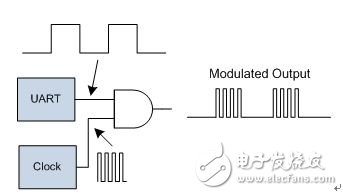
Figure 1 Simple modulated UART
AtmelXMEGA Custom Logic (XCL)The AtmelXCL module has two LUTs (look-up table) modules and two 8-bit timer/counter modules. The two LUTs do not have to be connected to the timer/counter module, but are interconnected with the UART, the EVENT module, or the IO pin. These two LUTs can be used as two separate 2-input units or as a single 3-input unit. The logic module can be configured as combinational logic such as AND, NAND, OR, NOR, XOR, XNOR, NOT, or MUX functions. They can also be configured as sequential logic functions, such as D flip-flops, D latches, or RS latches. Being able to interconnect with other logic blocks and IO pins, these simple LUT blocks can easily allow designers to avoid using some external logic or save CPU cycles. For example, the Atmel XCL Module Application Note (AT01084) explains how to configure the XCL module to avoid providing Manchester encoding for the UART output with additional CPU overhead or external logic. The AVRXMEGAE device has a built-in XCL module.
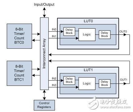
Figure 2 Atmel's XMEGA Custom Logic (XCL)
Microchip Configurable Logic Cell (CLC)MicrochipCLC allows users to select up to four signals from eight inputs. These inputs can be a combination of two IO pins, internal clocks, peripherals, or register bits. These four signals are then routed to the programmable logic module. The logic module can be programmed as one of 8 combinations of AND-OR, OR-XOR, 4-input AND, and SR latches. It can also be configured as one of 4 other combinations of flip-flops. Microchip gives some examples in its Application Note for Configurable Logic Unit Tips and Tricks. One of the examples demonstrates how to configure these modules to decode orthogonal signals. Without using these additional logic blocks, the CPU needs to sample the signal at a much higher rate to avoid spurious rotation of the signal that is in the transition phase, leaving the CPU interrupted only by a valid transition. The Microchip PIC10(L)F320/322 devices each contain a CLC module, and each CLC module contains four modules as shown in Figure 3.
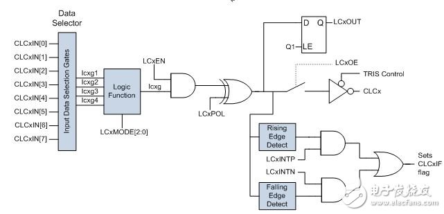
Figure 3 Microchip's Configurable Logic Cell (one of 4)
NXP pattern matching engineThe user-configurable logic provided by NXP is called the pattern matching engine. The logic module's input selects up to eight GPIO inputs. These eight inputs can generate product terms for complex Boolean expressions. These outputs can be used to trigger interrupts, drive special IO pins, or route to the next logic block or slice. Other features support rising or falling signals and edge detection of inverted signals. This additional hardware is configured to interrupt the CPU only if complex (or simple) event combinations occur. The NXPLPC81x device contains a pattern matching engine.
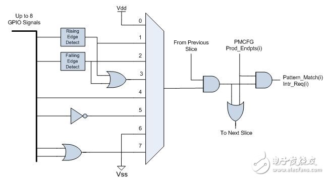
Figure 4 NXP pin interrupt/pattern matching engine
Cypress PSoC Universal Digital Block (UDB)Cypress is using a common digital module or UDB to use a more advanced approach to differentiate itself from the other three vendor methods described above and FPGAs. A UDB consists of two 12C4 PLDs and a data path. The PLD can be used to control the operation and data flow of the data path. It can also be used as a general-purpose logic and state machine. The data path is a custom module that provides 8-bit functions (AND, OR, ADD, SUB, INC, DEC, XOR), shift functions (left and right), and two 4-byte FIFOs for data queuing. These modules can also be combined to provide 16-bit, 24-bit or 32-bit functionality.
UDB inputs and outputs can be routed to any GPIO, peripheral/component IO, interrupt, etc. Interconnections between UDBs, fixed-function analog and digital modules, and GPIOs all use digital signal interface (DSI) processing. The UDB is programmed to perform any function, from simple logic gates to counter and PWM and universal serial interfaces such as UART and I2C peripherals.
For UDB implementation of the design, the user can choose from a variety of options. You can either place simple logic gates in schematics or implement designs in Verilog. A custom graphical interface is also available to enable design without the use of Verilog. The PSoC3, PSoC4, and PSoC5 family of microcontrollers can include from 4 to 24 such logic blocks (UDBs).
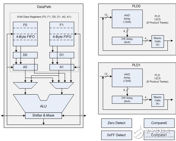
Figure 5 Cypress PSoC Universal Digital Block (UDB)
Custom interface instanceRecently I noticed that some RGB LEDs produced by Worldsemi are very interesting. The part numbers are WS2811, WS2812, and WS2812B, but they work in the same way. Only one GPIO pin is required, and you can drive 1,000 or more such components. This is quite interesting because I can control such a large number of RGB LEDs with one GPIO pin. The interface to connect these LEDs is not SPI, UART, or I2C but a custom interface. The communication signal uses asynchronous signals and each bit starts at the rising edge. Data 1 or 0 is determined by the high pulse length shown in the figure below.
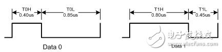
Figure 6 WS2811/12 data 0/1 timing
Each part requires 24 bits of data, and each color (red, green, blue) is 8 bits in the following format.

Figure 7 WS2811/12 data format
The WS2811/12 components use DIN (data input) and DOUT (data output) signals for simple serial connection. Each part retains the first 24 bits of data it sees, and then outputs the remaining data from the DOUT pin. See Figure 8 below.
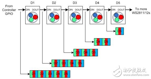
Figure 8 Connecting Multiple WS2811/12 Components
When the data flow starts, each part will see continuous data flow. If the rising edge of the data signal does not exceed 50 microseconds, the part latches the data, treats the next 24 bits of data as its own data, and retransmits the rest of the data.
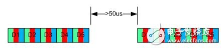
Figure 9 Device Reset When the Data Stream Is Idle for More Than 50 Microseconds
As you can see, the principle is not complicated, but it does not easily fit into standard microcontroller hardware. I do find that someone uses the SPI interface to maintain timing, but this requires that each real data bit uses at least three SPI data bits, which has little advantage in achieving CPU performance through bit debonding. Since the timing is not critical, if you implement the interface in the firmware (bit-slicing), the CPU will be dedicated to invert the drive signal until the LED is fully updated. This means that you need to disable all interrupts and not respond to any other input throughout the process. If you have 1,000 LEDs, the update time is (0.40 microseconds +0.85)*24 bits*1,000 LEDs=30,000 microseconds or 30 milliseconds. This may not be a problem, but if you want to update the LED at 30Hz, you will use almost 100% of the CPU!
When writing code, I'm used to avoid blocking code or conditions where I have to disable interrupts for a long time, especially if I have a user interface in the system or need to communicate with other processors. My goal is to minimize the CPU's burden and let the hardware do most of the work, just as the common internal UART or SPI module does today. Cypress PSoCUDB has several features that make this job very easy. Each UDB has two 4-byte FIFOs and a shifter in the data path. When implementing a UART, you can use one FIFO as a TX buffer and the other as an RX cache. For the WS2811/12, I only need one output FIFO and shifter. I decided to configure the hardware to generate an interrupt for each device at a time. The interrupt handler will load 24-bit (3-byte) data until the FIFO is empty. With this method, interrupts can be interrupted every 30 microseconds without having to disable all interrupts and bit tearing at 150 nanoseconds or less. The microcontroller I decided to use was the Cypress PSoCCY8C4245AXI. The bulk purchase price of the microcontroller is about one US dollar, four UDBs, and the operating frequency is 48 MHz, which is sufficient to meet the speed and hardware requirements for this task.
The design uses two of the four UDBs provided by PSoC. One is for using FIFO to buffer data and shift data so that all 24 bits (3 bytes) of each device can be written at one time. The second UDB can use two compare outputs to create a PWM. One compare output is used to create a logic 0 and the other is used to create a logic one. This serial data can be used to control the digital multiplexer and select waveform 1 or 0. See the block diagram in Figure 10 below.
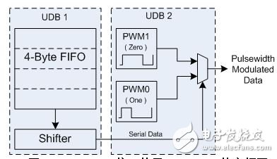
Figure 10 Block Diagram of WS2811/12 Interface Using PSoCU DB
Most product terms in UDB's four PLDs (two per UDB) can be used to control the data path, generate interrupts, provide status and control functions, but this also uses half of the UDB resources in this low-cost microcontroller. .
The next task is to clarify how much CPU overhead this design can save for the design. Taking an array of 1,000 LEDs as an example, the refresh rate is 30 Hz. If the design uses firmware to bit-slice the interface, it will consume almost 100% of the CPU resources. Using programmable hardware in the PSoC device can still do interrupts every 30 microseconds. Although this is a heavier load, the ARM Cortex-M0 running at 48 MHz is sufficient. To test the CPU overhead, I created a simple loop to refresh the monitor at about 30Hz. In the main loop, I triggered a pin and then used an oscilloscope to count the number of triggers in 40 milliseconds. Then I disable the interrupt, run the project again, and compare the results. Persistent display refresh consumes only about 12% of CPU resources compared to almost 100% of CPU usage caused by bit breaks in the firmware. This allows another 88% of the CPU cycles to be used for external communications and user interfaces. If you add DMA to your design, the overhead may drop from 12% to 2% or less. The cheapest PSoC I use (about $1) contains only UDB but no DMA, but some larger components do have built-in DMA.
I then produced a real RGB LED board consisting of a grid of 60x16 LEDs (960 LEDs) to test the component. The component operates as expected and can be used as a graphical interface for displaying basic lines, rectangles, circles, and text.
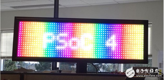
Figure 11 Billboards made using 960 RGB LEDs
Whether it is a large LED panel or a simple custom interface, some internal programmable hardware can have a significant impact on design performance. Not every custom interface requires multi-byte FIFOs or full hardware state machines, but having this kind of flexibility gives you more design choices, improved performance, or allows existing designs to quickly adapt to product requirements.
in accordance of the Voltage range of the inverter, the PV boards can be installed in series to meet the input voltage of inveter, and several such series to be installed in parallel, to input into the combiner. The current goes through lightenling protection and breaker equipment, then ouput for connection with inverter. We strongly suggest the users to follow all the necessery safety regulation, take all the safefy masures mentioned in the manual, to lower the possibility of danger, make sure of the personal safety.
PV Combiner Box 8in1outs,PV Combiner Box 16 In1outs,PV Combiner Box 30 In1outs,PV Combiner Box
Jinan Xinyuhua Energy Technology Co.,Ltd , https://www.xyhenergy.com