How many wafers can a wafer be cut? This is determined by the size of your die and the size of the wafer and the yield. In order to let everyone better understand this problem, before answering the question "How many wafers can a wafer be cut?", let's first take a look at the wafer fabrication process and the meaning of wafer, die, and chip. the difference.
Popular science: the difference between wafer die
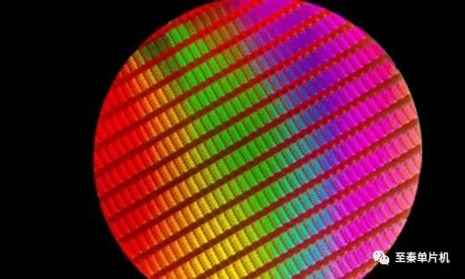
Let's start with a complete wafer (Wafer):
a complete wafer
Explanation of terms: wafer is the wafer shown in the picture, which consists of pure silicon (Si). Generally divided into 6-inch, 8-inch, and 12-inch specifications, the wafer is produced based on this wafer. A small piece on the Wafer is a wafer wafer body, named after the die, which becomes a particle after encapsulation. A wafer containing Nand Flash wafers, the wafer is first cut, then tested, and the intact, stable, full-capacity die is removed and packaged to form the Nand Flash chip that is seen everyday. Then, the rest on the wafer, or not, is unstable, or it is partially damaged, so it is not enough capacity, or it is completely damaged. The original factory considers the quality assurance, and will declare the death of this die, which is strictly defined as the scrapping of all waste products.
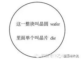
The relationship between die and wafer
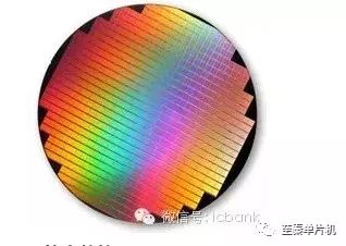
After the qualified die is cut, the original wafer becomes the picture below, which is to pick the remaining Downgrade Flash Wafer.
Filtered wafer
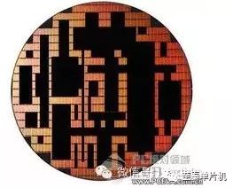
These residual die are actually wafers of unqualified quality. The part that is taken away, that is, the black part, is a qualified die, which will be packaged as a finished NAND granule by the original factory. The unqualified part, that is, the part left in the figure is treated as waste.
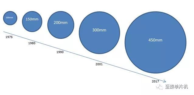
Wafer size development history
Wafer manufacturing process
The life course of an integrated circuit chip is the process of making sand into gold: the chip company designs the chip - the chip production factory produces the chip - the packaging and testing factory conducts the packaging test - the whole machine purchases the chip for the whole machine production.
Chip suppliers are generally divided into two categories: one is called IDM, and the popular understanding is the enterprise that integrates multiple industrial chain links such as chip design, manufacturing, packaging and testing. Some even have their own downstream machine parts, such as Intel, Samsung, IBM is a typical IDM enterprise.
Another type, called Fabless, is a chip supplier that does not have a chip processing factory. Fabless designs, develops and markets its own chips, and outsources its production-related business to professional manufacturers such as Qualcomm, Broadcom, MediaTek, and Spreadtrum.
Corresponding to Fabless is Foundry and the testing and testing plant. It mainly undertakes the production and packaging testing tasks of Fabless. Typical Foundry (such as TSMC, Groffont, SMIC, Taiwan) UMC, etc., the seal test factory has ASE, Jiangsu Changdian and so on.
How many wafers can a wafer be cut?
The so-called 6-inch, 12-inch or 18-inch wafers in the industry are actually short for wafer diameter, but this is an estimate. The actual wafer diameter is divided into three types: 150mm, 300mm, and 450mm, and 12å‹ is equal to 305mm. It is called a 12-inch wafer for convenience.
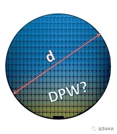
The general calculation formula of the international Fab factory:

Smart readers must have found that the square of π* (wafer diameter/2) in the formula is not the formula of the circular area? If you simplify the formula, it will become:

X is the so-called dpw die per wafer .
Then come to test your computing skills!
Assuming that the 12-inch wafer costs $5,000 per piece, NVIDIA's latest GT200 wafer size is 576 square millimeters. At a yield of 50%, what is the average cost per dollar?
Hf Drivers - Neodymium,Bullet Tweeter Speaker,Loud And Ultra Crisp Sound,Compression Driver
NINGBO BOILINGSOUND ELECTRONICS CO.,LTD , https://www.tweeterspeaker.com