In this article, I'll delve into the buck, boost, and buck-boost topologies in different ways.
Buck converter
Figure 1 is a schematic diagram of a non-synchronous buck converter. The buck converter reduces its input voltage to a lower output voltage. When switch Q1 is turned on, energy is transferred to the output.
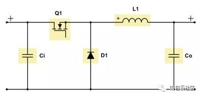
Figure 1: Schematic of a non-synchronous buck converter
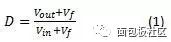
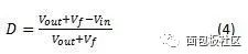
Equation 1 calculates the duty cycle:
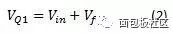
Equation 2 calculates the maximum metal oxide semiconductor field effect transistor (MOSFET) stress:
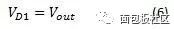
Equation 3 gives the maximum diode stress:
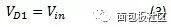
Where Vin is the input voltage, Vout is the output voltage, and Vf is the diode forward voltage.
The greater the difference between the input voltage and the output voltage compared to a linear regulator or a low dropout regulator (LDO), the higher the efficiency of the buck converter.
Although the buck converter has a pulsed current at the input, the output current is continuous because the inductor-capacitor (LC) filter is at the output of the converter. As a result, the voltage ripple reflected to the input will be larger than the ripple at the output.
For buck converters with small duty cycles and output currents greater than 3A, synchronous rectifiers are recommended. If your power supply requires more than 30A of output current, it is recommended to use multiphase or interleaved power stages as this minimizes component stress, dissipates the generated heat between multiple power stages, and reduces reflection at the input of the converter. Ripple.
The use of an N-FET results in a limited duty cycle because the bootstrap capacitor needs to be recharged in each switching cycle. In this case, the maximum duty cycle is in the range of 95-99%.
Buck converters typically have good dynamics because they are forward topologies. The achievable bandwidth depends on the quality of the error amplifier and the selected switching frequency.
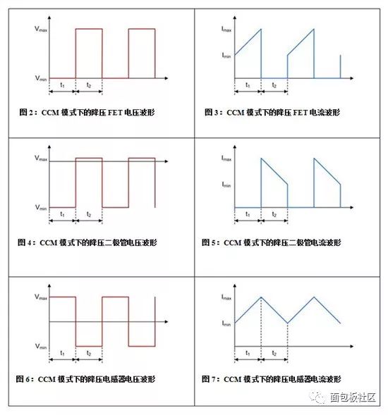
Figures 2 through 7 show the voltage and current waveforms of FETs, diodes, and inductors in continuous conduction mode (CCM) in a non-synchronous buck converter.
Boost converter
The boost converter boosts its input voltage to a larger output voltage. When switch Q1 is not conducting, energy is transferred to the output. Figure 8 is a schematic diagram of a non-synchronous boost converter.
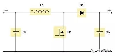
Figure 8: Schematic diagram of the non-synchronous boost converter
Equation 4 calculates the duty cycle:
Equation 5 calculates the maximum MOSFET stress:

Equation 6 gives the maximum diode stress:
Where Vin is the input voltage, Vout is the output voltage, and Vf is the diode forward voltage.
Using the boost converter, you can see the pulse output current because the LC filter is at the input. Therefore, the input current is continuous and the output voltage ripple is greater than the input voltage ripple.
When designing a boost converter, it is important to know that even if the converter is not switching, there will be a permanent connection from input to output. Precautions must be taken to prevent possible short-circuit events at the output.
For output currents greater than 4A, a synchronous rectifier should be used instead of a diode. If the power supply needs to provide an output current greater than 10A, it is highly recommended to use a multi-phase or interleaved power stage approach.
When operating in CCM mode, the dynamics of the boost converter are limited due to the right half plane zero (RHPZ) of its transfer function. Since the RHPZ cannot compensate, the achievable bandwidth will typically be less than one-fifth to one-tenth of the RHPZ frequency. See Equation 7:
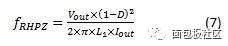
Where Vout is the output voltage, D is the duty cycle, Iout is the output current, and L1 is the inductance of the boost converter.
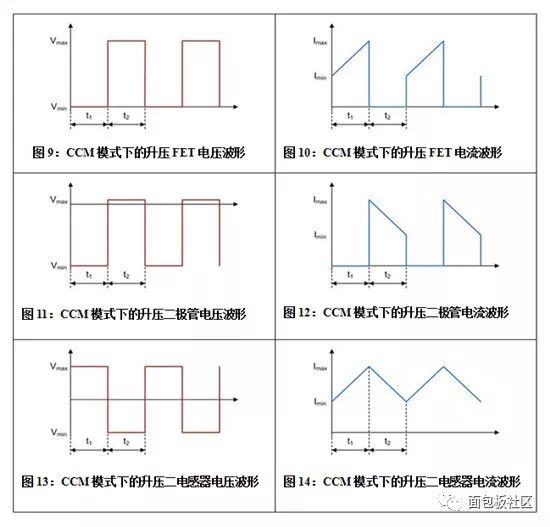
Figures 9 through 14 show the voltage and current waveforms of the FET, diode, and inductor in CCM mode in a non-synchronous boost converter.
Buck-boost converter
The buck-boost converter is a combination of buck and boost power stages that share the same inductor. See Figure 15.

Figure 15: Schematic of a dual-switch buck-boost converter
The buck-boost topology is practical because the input voltage can be smaller, larger, or the same than the output voltage, requiring an output power greater than 50W.
For output powers less than 50W, the single-ended primary inductor converter (SEPIC) is a more cost-effective option because it uses fewer components.
When the input voltage is greater than the output voltage, the buck-boost converter operates in buck mode; when the input voltage is less than the output voltage, it operates in boost mode. When the converter is operating in a transmission region where the input voltage is within the output voltage range, there are two concepts to deal with these situations: either the buck and boost stages are active at the same time, or the switching cycle is between the buck and boost stages. Alternately, each typically runs at half the normal switching frequency. The second concept can cause subharmonic noise at the output, and the output voltage accuracy may be less accurate than conventional buck or boost operation, but the converter will be more efficient than the first concept.
The buck-boost topology has pulsed currents at both the input and output because there is no LC filter in either direction.
For buck-boost converters, buck and boost power stage calculations can be used separately.
The buck-boost converter with two switches is suitable for power ranges from 50W to 100W (such as the LM5118) and synchronous rectification power up to 400W (same as the LM5175). It is recommended to use a synchronous rectifier with the same current limit as the uncompressed buck and boost power stages.
You need to design a compensation network for the buck-boost converter for the boost stage because RHPZ limits the regulator bandwidth.
25 Ft Ethernet Cable,Ethernet Cable Cat 6,Best Lan Cable,75 Ft Ethernet Cable
Zhejiang Wanma Tianyi Communication Wire & Cable Co., Ltd. , https://www.zjwmty.com