FPGA designers strive to achieve higher performance while meeting critical timing margins. In this case, the design of memory interfaces has always been a difficult and time-consuming challenge. Xilinx FPGA provides I/O modules and logic resources to make interface design simpler and more reliable. Nevertheless, I/O modules and additional logic still need to be configured, verified, executed by the designer in the source RTL code, and correctly connected to the rest of the FPGA, after careful simulation, and then verified in hardware to ensure the memory interface The reliability of the system.
This white paper discusses the challenges faced by various memory interface controller designs and Xilinx’s solutions. It also explains how to use Xilinx software tools and hardware-proven reference designs for your own applications (from low-cost DDR SDRAM applications to (Higher performance interface like 667 Mb/sDDR2 SDRAM) design complete memory
Storage interface solutions.
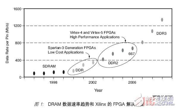
Memory interface trends and Xilinx solutionsIn the late 1990s, the memory interface developed from single data rate (SDR) SDRAM to double data rate (DDR) SDRAM, and today's DDR2 SDRAM runs at 667 Mb/s per pin or higher. Current trends show that these data rates may double every four years, and by 2010, with the advent of DDR3 SDRAM, it is likely to exceed 1.2 Gb/s per pin. see picture 1.
Applications can generally be divided into two categories: one is low-cost applications, with the main purpose of reducing device cost; the other is high-performance applications, the primary goal is to seek high bandwidth.
DDR SDRAM and low-end DDR2 SDRAM that run at a speed lower than 400 Mb/s per pin can already meet the bandwidth requirements of most low-cost system memories. For this type of application, Xilinx offers the Spartan-3 series of FPGAs, which include Spartan-3, Spartan-3E and Spartan-3A devices.
High-performance applications push memory interface bandwidths such as 533 and 667 Mb/s DDR2 SDRAM to the limit; for this type of application, Xilinx has introduced Virtex-4 and Virtex-5 FPGAs, which can fully meet the requirements of most systems today. Highest bandwidth requirement.
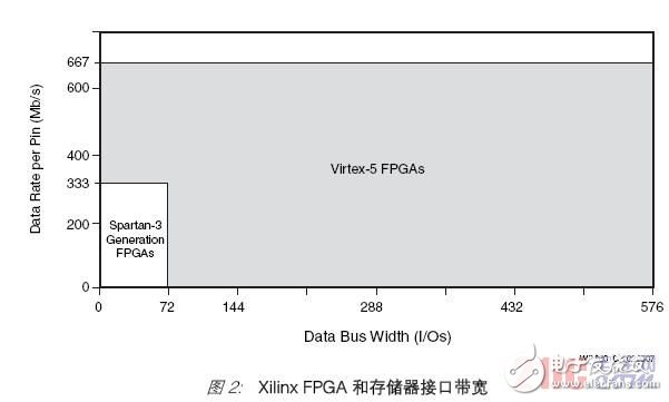
Bandwidth is a factor related to the data rate per pin and the width of the data bus. The Spartan-3 series, Virtex-4, and Virtex-5 FPGAs provide different options, from smaller low-cost systems with data bus widths less than 72 bits,
To a larger Virtex-5 package with a width of 576 bits (see Figure 2).
The wider bus at speeds higher than 400 Mb/s makes the chip-to-chip interface more difficult to develop because of the need for larger packages, better power and ground-to-signal ratios. The development of Virtex-4 and Virtex-5 FPGAs uses advanced Sparse ChevrON (Sparse ChevrON) packaging technology to provide excellent signal-to-power and ground pin ratios. There are enough power and ground pins and boards around each I/O pin to ensure good shielding and minimize crosstalk noise caused by Synchronous Switching Output (SSO).
Low-cost memory interfaceToday, not all systems are pursuing the performance limits of memory interfaces. When low cost is the main determinant, and the bit rate of the memory is enough to reach 333 Mb/s per pin, Spartan-3 series FPGA with Xilinx software tools can provide an easy-to-implement, low-cost solution .
FPGA-based memory interfaces and controllers are composed of three basic building blocks: a read-write data interface, a memory controller state machine, and a user interface that bridges the memory interface design to the rest of the FPGA design (Figure 3). These modules are implemented in FPGA resources and are driven by the output of the Digital Clock Manager (DCM) as a clock. In the Spartan-3 series implementation, the DCM also drives a look-up table (LUT) delay calibration monitor (a logic block that ensures the correct timing of read data acquisition). The delay calibration circuit is used to select the number of delay cells based on the LUT, and these delay cells are used to delay the strobe line (DQS) for the read data. The delay calibration circuit calculates the delay of the same circuit as the DQS delay circuit. All delay factors will be considered during calibration, including all component and wiring delays.
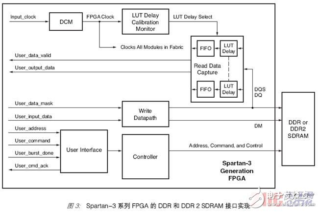
The user interface is a handshake type interface. The user issues a read or write command, if it is a write command, it also includes the address and data, and the user interface logic responds with the User_cmd-ack signal, so the next command can be issued.
In the implementation of the Spartan-3 series, the LUT in the configurable logic block (CLB) is used to realize the read data collection. During a read transaction, the DDR or DDR2 SDRAM device sends the read data strobe (DQS) and related data to the FPGA in a manner aligned with the edge of the read data (DQ). Collecting and reading data in a source-synchronous interface running at a high frequency is a challenging task because the data changes on each edge of the non-free running DQS. The realization of read data collection uses a tap delay mechanism based on LUT. The DQS clock signal is delayed by an appropriate amount, so that it has enough margin in the valid window of the read data after it is placed, so that it can be collected in the FPGA.
The collection of read data is completed in the LUT-based dual-port distributed RAM (see Figure 4). The LUT RAM is configured as a pair of FIFOs, and each data bit is input to the FIFO of the rising edge (FIFO 0) and the falling edge (FIFO 1), as shown in Figure 4. These 16-input FIFOs run asynchronously and have independent read and write ports.
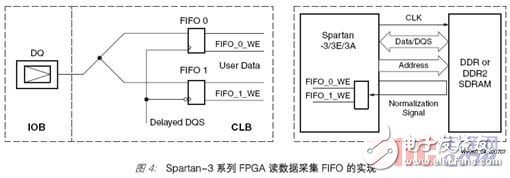
The read data from the memory is written to FIFO_0 on the rising edge of the delayed DQS, and written to FIFO_1 on the falling edge of the delayed DQS. The transfer of read data from the DQS clock domain to the memory controller clock domain is accomplished through these asynchronous FIFOs. In the clock domain of the memory controller, data can be read from FIFO_0 and FIFO_1 at the same time. The read pointer of the FIFO is generated in the internal clock domain of the FPGA. The generation of write enable signals (FIFO_0 WE and FIFO1_WE) is completed by DQS and an external loopback (ie normalization) signal. The external normalized signal is sent as an output to the input/output module (IOB), and then taken out as an input through the input buffer. This technique can compensate for IOB, device, and trace delays between the FPGA and the memory device. The normalized signal sent from the FPGA input pins uses similar wiring as DQS before entering the LUT delay circuit
Resources to match the routing delay. The trace delay of the loop should be the clock sent to the memory and the trace of DQS
The sum of the delays (Figure 4).
The write data command and timing are generated and controlled by the write data interface. The write data interface uses the 90-degree, 180-degree, and 270-degree outputs of the IOB flip-flop and DCM, and sends DQS that is correctly aligned with the command and data bits according to the timing requirements of DDR and DDR2 SDRAM.
The implementation of a DDR and DDR2 SDRAM memory interface for Spartan-3 series FPGAs has been fully verified by hardware. A low-cost DDR2 SDRAM reference design example using the Spartan-3A starter kit has been completed. This design is developed for on-board 16-bit wide DDR2SDRAM memory devices and uses XC3S700A-FG484. This reference design utilizes only a small part of the available resources of the Spartan-3A FPGA device: 13% of the IOB, 9% of the logic slice, 16% of the BUFG MUX, and one of the eight DCMs. This implementation leaves available resources for other functions required by the rest of the FPGA design.
Using the memory interface generator (MIG) software tool (explained later in this white paper), designers can easily customize the memory interface design of the Spartan-3 series to suit their applications.
High-performance memory interfaceAs data rates increase, it becomes more and more difficult to meet interface timing requirements. Compared with writing to the memory, when reading data from the memory, the requirements for the clock control of the memory interface are usually more difficult to meet. The trend of pursuing higher data rates makes designers face a huge challenge, because the data valid window (this is a period of time in the data cycle during which reliable data can be read) shrinks faster than the data cycle itself. The reason for this is that the system and device performance parameters that affect the size of the effective data window have various uncertainties, and their shrinking rate is different from the data period.
If you compare the data valid window of the DDR SDRAM running at 400 Mb/s with the running speed of 667
Mb/s DDR2 memory technology, this situation is clear at a glance. A DDR device with a data period of 2.5 ns has a data valid window of 0.7 ns, while a DDR2 device with a data period of 1.5 ns has a data valid window of only 0.14 ns (Figure 5).
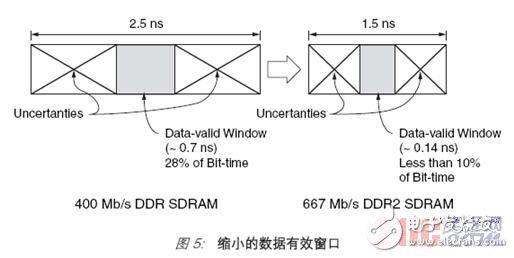
Obviously, the accelerated reduction of the data valid window has brought a bunch of new design challenges to FPGA designers. To create and maintain reliable memory interface performance, more effective methods must be adopted.
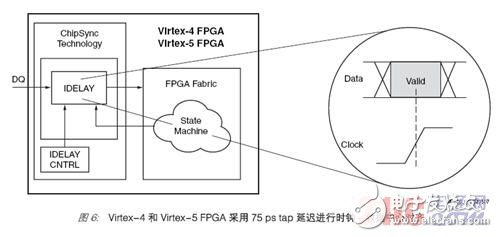
As implemented in the Spartan-3 series of FPGAs, the read data can be collected into a configurable logic block (CLB) by using the read data DQS, but when the LUT is used to align the DQS or clock with the center of the data valid window, the delay used is tap It's very rough. The delay tap implemented in CLB has a resolution of about a few hundred picoseconds (ps), however, for read acquisition timings with data rates exceeding 400 Mb/s, the required resolution is an order of magnitude higher than that of CLB-based taps . Virtex-4 and Virtex-5 FPGAs use dedicated delay and clock resources in I/O modules (called ChipSync? technology) to solve this problem. The ChipSync module built into each I/O contains a series of delay units (tap delay), called IDELAY in Virtex-4, and IODELAY in Virtex-5FPGA, with a resolution of 75 ps (see figure 6).
The architecture of this implementation is based on several building blocks. The user interface is responsible for bridging the memory controller and physical layer interface to the rest of the FPGA design, and it uses the FIFO architecture (Figure 7). There are three sets of FIFO: command/address FIFO, write FIFO, and read FIFO. These FIFOs hold commands, addresses, write data and read data. The main controller module controls read, write and refresh operations. The other two logic modules perform clock-data center alignment for read operations: initialize the controller and calibrate the logic.
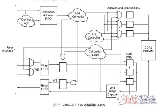
The physical layer interface for address, control and data is implemented in the I/O module (IOB). The read data is recollected in the second stage of the latch (which is also part of the IOB).
The Virtex-4 and Virtex-5 FPGA memory interface reference designs support two read data acquisition techniques. The direct clock technology supported by Virtex-4FPGA delays the read data, so the system clock in the input DDR flip-flop using IOB can directly register the read data. In order to align the FPGA clock to the best state, each read data bit will be individually verified. This technique provides sufficient performance for clock rates up to 240 MHz.
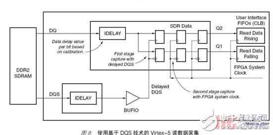
The second technology is called DQS-based technology. This technology is used for higher clock rates, and both Virtex-4 and Virtex-5FPGA support this technology. It uses the memory DQS to collect the corresponding read data, and the data is
The delayed signal (distributed through a local I/O clock buffer (BUFIO)) is registered. This data is then triggered
The second stage of the device is synchronized with the clock domain of the system. The input serializer/deserializer function in IOB is used for reading data acquisition; the first pair of flip-flops transfer data from the delayed DQS domain to the system clock domain (Figure 8).
Both technologies involve the application of tap delay (IDELAY) units, and these delay units will vary in the verification program implemented by the verification logic. During system initialization, this calibration procedure is performed to set the optimal phase between DQS, data, and system clock. The purpose of this is to maximize the timing margin. Calibration eliminates any uncertainty caused by process-related delays, thereby compensating for those path delay components that are constant for any circuit board. These components include PCB trace delays, package delays, and process-related propagation delay components (both in memory and FPGA), and setup/hold time of acquisition triggers in FPGA I/O modules. Some delays are determined by the process, voltage and temperature of the system initialization phase, and calibration is responsible for solving these delay changes.
In the calibration process, the delay tap of DQS and data will be increased to perform edge detection. The detection method is to continuously read back data from the memory and sample the pre-programmed training mode or the memory DQS itself until the data strobe (DQS) is determined. The leading edge or the front and rear edges. Then the tap number of data or DQS is set to provide maximum timing margin. For “DQS-based†acquisition, DQS and data can have different tap delay values, because
Synchronization is essentially divided into two stages: one first collects data in the DQS domain, and the other transfers this data to the system clock domain.
At higher clock frequencies, the "DQS-based" acquisition method becomes very necessary. Its two-stage method can provide better acquisition timing margin, because the uncertainty of DDR timing is mainly limited to the first trigger of the IOB. One level. In addition, because DQS is used to register data, compared with clock-data (Tac) changes, the timing uncertainty of DQS-data changes is smaller. For DDR2, for example, these uncertainties are given by the tDQSQ and tQHS parameters of the device.
As implemented in the Spartan-3 series of FPGAs, the write timing of Virtex-4 and Virtex-5 FPGAs is supported by the DCM, which generates the two-phase output of the system clock. The DQS of the memory is output by an output DDR register, which is driven by the non-inverted clock of the system clock. Write data is clocked by a DCM clock output 90° ahead of the system clock. This technique ensures that in the output part of the FPGA, the DQS is aligned with the data center of the write operation.
Other aspects of this design include the logic generation and user interface of the overall controller state machine. In order to make it easier for designers to complete the entire design, Xilinx has developed a memory interface generator (MIG) tool.
Controller design and integrationCreating a memory controller is an extremely complex and delicate task. To solve the problems faced by FPGA designers, they need tools that come with the FPGA to provide a newer level of integration support.
For the integrity of the design, it is necessary to integrate all the building blocks including the memory controller state machine. The controller state machine differs depending on the memory architecture and system parameters. State machine coding can also be very complicated, it is a function of multiple variables, for example:
Architecture (DDR, DDR2, QDR II, RLDRAM, etc.)
Number of banks (outside or inside the memory device)
Data bus width
The width and depth of the memory device
Group and row access algorithm
Finally, the data-to-DQS ratio (DQ/DQS) such parameters will further increase the complexity of the design. The controller state machine must issue commands in the correct order, while also considering the timing requirements of the memory device.
Use MIG software tools to generate a complete design. This tool is available as part of the CORE Generator reference design and intellectual property suite, which is freely available from Xilinx. The MIG design flow (Figure 9) is very similar to the traditional FPGA design flow. The advantage of the MIG tool is that it is no longer necessary to generate RTL code from scratch for the physical layer interface or memory controller.
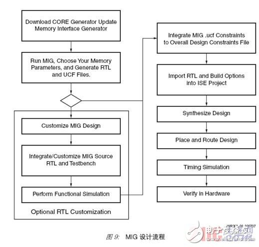
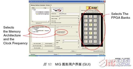
The MIG Graphical User Interface (GUI) can be used to set system and memory parameters (Figure 10). For example, after selecting the FPGA device, packaging method, and speed level, the designer can choose the memory architecture and choose the actual memory device or DIMM. The same GUI can also be used to select bus width and clock frequency. At the same time, for some FPGA devices, it also provides the option of having more than one controller to meet the requirements of multiple memory bus interfaces. Other options provide control over the clock control method, CAS delay, burst length, and pin assignment.
In less than a minute, the MIG tool can generate RTL and UCF files, the former is the HDL code file, and the latter is the constraint file. These files are generated using a hardware-verified reference design library and modified based on user input.
Designers enjoy complete flexibility to further modify the RTL code. Unlike other solutions that provide a "black box" implementation method, the code in this design is not encrypted, and the designer is completely free to modify and further customize the design. The output files are classified by modules, which are applied to the different building blocks of the design: user interface, physical layer, controller state machine, and so on. Therefore, the designer can choose to customize the state machine that controls the group access algorithm. The group access algorithms of Virtex-4 and Virtex-5 DDR2 generated by the MIG tool are different from each other. The Virtex-5 design uses a Least Recently Used (LRU) algorithm to make up to four groups of one line always open to reduce the overhead caused by opening/closing lines. If a row needs to be opened in a new group, the controller will close the row in the least recently used group and open a row in the new group. In the Virtex-4 controller implementation, only a single group has an open row at any time. Each application may need its own access algorithm to maximize throughput. Designers can modify the algorithm by changing the RTL code to better suit the access mode of their application.
After modifying the optional code, the designer can perform simulation again to verify the function of the overall design. The MIG tool can also generate a comprehensive test platform with memory verification function. The test platform is a design example for functional simulation and hardware verification of Xilinx basic design. The test platform issues a series of write and read back commands to the storage controller. It can also be used as a template to generate a custom test platform.
The final stage of the design is to import the MIG files into the ISE project, merge them with the rest of the FPGA design files, then perform synthesis, placement and routing, and if necessary, run other timing simulations, and finally perform hardware verification. The MIG software tool will also generate a batch file, including the corresponding synthesis, mapping, and placement and routing options to help optimize the generation of the final bit file.
High-performance system designThe realization of high-performance memory interface is far more than the realization of FPGA on-chip design, it needs to solve a series of chip-to-chip problems, such as the requirements for signal integrity and the challenges of circuit board design.
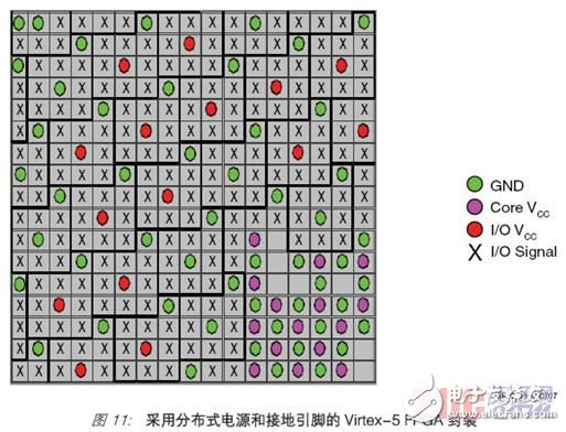
The challenge of signal integrity is to control crosstalk, ground bounce, ringing, noise tolerance, impedance matching and decoupling to ensure a reliable signal effective window. The column architecture used by Virtex-4 and Virtex-5 FPGAs enables I/O, clock, power, and ground pins to be deployed anywhere on the chip, not just along the periphery. This architecture alleviates issues related to I/O and array dependencies, power and ground distribution, and hard IP expansion. In addition, the sparse zigzag packaging technology used in Virtex-4 and Virtex-5 FPGAs can evenly distribute power and ground pins throughout the package. These packages provide better crosstalk immunity and improve signal integrity in high-performance designs. Figure 11 shows the Virtex-5 FPGA package pins. The dots represent the power and ground pins, and the crosses represent the pins available to users; in this layout, the I/O signal is surrounded by enough power and ground pins to ensure effective shielding of SSO noise.
For high-performance memory systems, increasing the data rate does not always meet the demand; to achieve the desired bandwidth, a wider data bus is required. Today, 144 or 288-bit interfaces are everywhere. Simultaneous switching of multiple bits can cause signal integrity problems. The restriction on SSO is specified by the device supplier's trademark, which represents the number of signal pins in the device that the user can use for each group at the same time. With the good SSO noise shielding advantages of the sparse zigzag packaging technology and the homogeneous I/O structure, a wide data bus interface is completely possible.
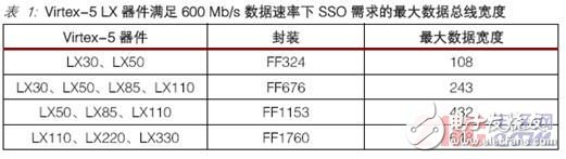
Table 1 lists the Virtex-5 LX devices and the maximum data bus width that meets the SSO requirements at a data rate of 600 Mb/s.
Another challenge in designing large-capacity or dense memory systems is the capacity load. High-performance memory systems may require multiple memory devices driven by a single bus shared by address and command signals. The high-capacity unbuffered DIMM interface is an example. If each single-rank DIMM has 18 components, an interface containing two 72-bit unbuffered DIMMs can have up to 36 receivers on the address and command buses. The maximum load recommended by the JEDEC standard and common in general-purpose systems is two unbuffered DIMMs. The capacity load generated on the bus will be extremely large, leading to more than one clock cycle for the rising and falling of the signal edge, which makes the establishment and maintenance of the memory device wrong. Figure 12 shows the eye diagram provided by the IBIS simulation, using a different configuration: a register
DIMM, one unbuffered DIMM, and two single-rank unbuffered DIMMs. The capacity load ranges from 2 receivers when using registered DIMMs to 36 receivers when using unbuffered DIMMs.
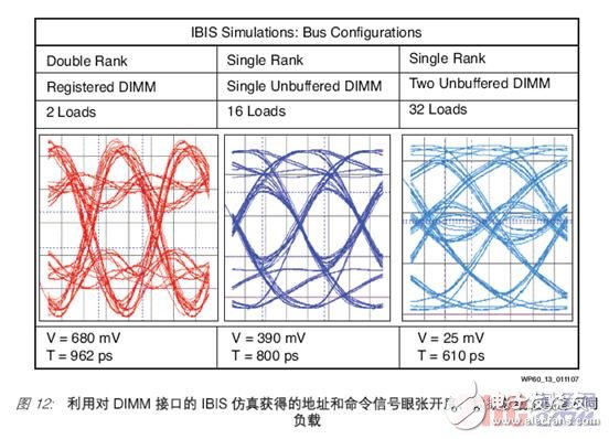
These eye diagrams clearly show the capacity loading effect of the address bus; register DIMMs provide a wide open window of validity on the address and command buses. The eye opening of a DIMM is still good at 267 MHz. However, when the load is 32, the effective window of the address and command signals is greatly reduced, and the traditional implementation method is no longer sufficient to reliably interface with two unbuffered DIMMs.
This simple test example shows that the load will cause the edge to slow down significantly while the eye diagram is closed at a higher frequency. For systems where the bus load cannot be reduced, reducing the operating clock frequency can be a way to maintain signal integrity at an acceptable level. However, there are other ways to solve the capacity load problem without reducing the clock frequency: In applications where one clock cycle delay can be added to the interface, the use of registered DIMMs can be a good choice. These DIMMs use a register to buffer signals such as addresses and commands, thereby reducing capacity load. Using a design technique based on the use of two clock cycles (called 2T timing) on ​​the address and command signals, the address and command signals can be sent at half the system clock frequency. Controlling the cost of a memory system is the same as achieving the required performance, which is also a big challenge. One way to reduce the complexity of circuit board design and reduce material costs is to use on-chip terminals instead of resistors on the circuit board. Virtex-4 and Virtex-5 series FPGAs provide a function called "Digitally Controlled Impedance (DCI)", which can be implemented in the design to reduce the number of resistors on the circuit board. The MIG tool has a built-in option that allows designers to include the above functions for address, control, or data buses when implementing memory interface designs. A trade-off factor to be considered at this time is when the terminal is implemented on-chip, which is better than off-chip power consumption.
Development board for memory interfaceHardware verification of the reference design is an important final step to ensure that the solution is rigorous and reliable. Xilinx has verified the memory interface design of the Spartan-3 series, Virtex-4 and Virtex-5 FPGAs. Table 2 shows the supported memory interfaces for each development board.
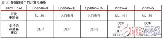
The range of development boards covers from low-cost Spartan-3 series FPGA implementations to the high-performance solutions provided by Virtex-4 and Virtex-5FPGA series devices.
in conclusionWith suitable FPGAs, software tools and development boards, the design of memory interface controllers using 667 Mb/s DDR2SDRAM has become a fast and smooth process, whether it is a low-cost application or a high-performance design. Finished handily.
Liquid Crystal Display,Lcd Screen Displays,Calculator Lcd Display,Lcd Display For Car Bluetooth
Dongguan Yijia Optoelectronics Co., Ltd. , https://www.everbestlcdlcm.com