Overview
The Real Time Clock Chip (RTC) allows a system to synchronize or log events, giving the user an easy-to-understand time reference. Due to the increasing use of RTCs, designers should be familiar with RTCs in order to avoid problems in design.
Select interface
The range of bus interfaces available to RTC is wide. The serial interface includes 2-wire (I2C), 3-wire and serial peripheral interface (SPI). The parallel interface consists of multiple buses (multiple data and address lines) and designs with separate address and byte data inputs. The choice of interface is usually determined by the type of processor used, and many processors include 2-wire or SPI interfaces. Others, such as the 8051 processor and its derived processors support multiple address and data buses. Time Keeping Non-Volatile (NV) RAM and SRAM use the same control signals, and many processors offer this convenient interface, as well as a variety of different battery-backed RAMs. Finally, the invisible clock hides the battery-backed RAM and can be accessed using a 64-bit software protocol.
Backup battery function
In some applications, such as VCRS, if the power is removed, the time and date information will be lost. In many new applications, even if the main power supply is removed, the time and date information should be valid. In order to keep the clock crystal running, use a main or backup power supply, or a large capacity capacitor. In this case, the clock chip must be able to switch between the two power supplies.
If a battery, such as a button-type lithium battery, is used as the backup power source, the RTC should be designed to consume as little power as possible when operating with the backup power source. The power switching circuit, which is normally powered by the main power supply, causes the power supply to switch to battery power and puts the RTC into a low power mode. Communication between the microprocessor and the RTC is typically locked (called write protection) to minimize battery current and prevent data corruption.
Many clock chips include a crystal control bit, commonly referred to as a clock interrupt (CH) or a crystal enable bit (/EOSC). This bit is usually located in the highest bit of the second register or control register (bit 7). In almost all clock chips with this, the preferred state on the initial battery is not valid for the crystal. This allows the system designer to propose a manufacturing process that is powered by Vbat after installation and testing, usually with a lithium battery. At this point, the crystal oscillator is in a stopped state, and saving the battery to the system voltage can work. At this point, the software/hardware should start the crystal and cause the processing time and date.
In general, the operating temperature of a lithium battery is -40 ° C to +85 ° C. The battery should not be exposed to temperatures above +85 °C. Packages containing batteries and exposed batteries, such as sensitive sockets, should not be exposed to water. Immersion of water causes the battery to be shorted, thus draining the battery.
Clock module, unsealing and saving period
In standby battery mode, the current consumption of the clock is mainly from the crystal. All clock modules with embedded crystals and battery packs are already formed at the factory and the crystals are not working. When the crystal oscillator is not working, the current of the battery is less than the self-discharge current, or 0.5% of the annual temperature.
Some time keeps the non-volatile (NV) RAM module using a clock control IC and an SRAM. When they come out of the factory, the crystal oscillator does not work and the battery supplies power to the SRAM is discontinuous. After the VCC is removed for the first time, the battery is connected to the SRAM. This function is often referred to as “unsealing†and is used to save the battery until the module is first used. Other time to keep the non-volatile (NV) RAM module is a monolithic integrated circuit (with controller and SRAM in one IC), no need to unblock.
Module package
Time keeps non-volatile (NV) RAM, multiple bus clocks, some watchdogs and stealth clocks can be used for module or power cap packages. A 32.768Hz crystal and a lithium battery are embedded inside the module, making it easier to design the PCB. However, the crystal and battery cannot withstand the temperature during reflow. After reflowing, the module can be attached or inserted by hand onto the nest. As long as the lithium battery is not exposed to temperatures above 85 ° C, the module can also be soldered to the PCB by wave soldering.
The power cap product uses a two-piece construction to provide a surface soldering device that can be reflowed. The bottom of the module containing RAM and clock can be mounted to the board using standard reflow techniques. After soldering, the upper part of the power cap containing the sensitive battery and crystal will suddenly break to the bottom.
Clock format
RTC uses three main data formats, BCD format, binary format with separate registers such as month, week, year, and unformatted binary sender format.
BCD is one of the most commonly used formats. One reason it is popular is that time and date data can be easily read without conversion. Each 8-bit register represents two digits (one half digit per digit), and each 4-bit binary represents the digits 0 through 9. Figure 1 shows a typical binary clock format diagram.
Because some bits are not needed in special time or date fields, these bits can be used for special functions, generally used as read/write bits, or can be read back in hardware and always in the 1 or 0 state. This is determined by the design. In Figure 1, the seventh bit of the second register is used as the clock interrupt bit (CH).
The second is a binary form, and each individual register is the same as the BCD format. The binary format on a clock with BCD format is usually programmable.
The third is to use a single multibyte register to represent the second time in the unformatted binary value of a reference point.
Figure 1. Typical time and date register map
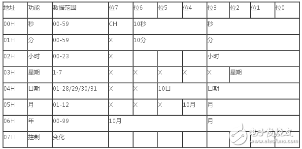
The time and date registers are updated every second. The value of the date varies depending on the year in which the month and February are located. The day of the week register is independent of other registers except the multi-bus clock. The week register increases at midnight and changes from 7 to 1. As long as the assignments in the program are continuous, the programmer can select any special day as "1". In the bus multiplexed clock, Sunday must be "1" because the week register saves the test with daylight. On the previous midnight change, the test saved for the day was completed at midnight, which must be stated when testing the daytime save function.
When the clock format is formatted from 12 hours to 24 hours, or from BCD to binary, or from binary to BCD, the time, date, and alarm registers must be reinitialized.
The unformatted binary counter clock has a separate register, typically 32 bits, which can be incremented once per second. Typically, the register value 00H is considered to be some default time or date value. For example, January 1, 1970, 00:00:00 is "0 o'clock". The binary value in the register represents the time elapsed from that point. Software programs must turn 32-bit binary values ​​into readable and writable times and dates, and convert user data into binary values.
Y2K Compliance
FS Semiconductor RTCs are compatible with Y2K, are Y2K compliant, or do not include date sensitive logic. A Y2K-compliant clock has these logics, including century information (with century numbers or century), which can correctly calculate leap years until 2099, but requires system software to track the century. The binary seconds clock has no date-sensitive logic, and the software must calculate the correct date, including the correctness of the leap year.
Crystal and accuracy
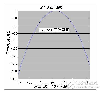
A crystal is one of the most accurate circuits that can be used to provide a fixed frequency. A 32768 Hz crystal is used for most RTCs. By dividing the output frequency of the crystal, a 1HZ reference frequency can be used to update the time and date. The accuracy of the clock is mainly determined by the accuracy of the crystal. The tuned crystal has a parabolic response to temperature (Figure 2). The 23 ppm error is approximately one minute per month.
Under special capacitive loads, the crystal oscillator can be tuned to the correct frequency. In an RTC designed to provide a crystal with a 6pF capacitive load, a crystal with a capacitive load of 12.5pF will cause the RTC to go faster.
Figure 2. Crystal Accuracy and Temperature
Crystal connection
There is a bias network inside all FS RTCs. The crystal should be connected directly to the pins of X1 and X2 without any other components (Figure 3). The crystal should be as close as possible to the X1 and X2 pins. The ground plane should be placed under the crystal, below X1 and X2 (Figure 4). The digital signal line should be away from the crystal and crystal pins, and components with severe radiated RFI should be shielded and away from the crystal. The low-power crystal oscillator circuit is sensitive to nearby RFI, and the RFI causes the clock to go faster.
Figure 3. The RTC-equivalent circuit shows its internal bias network
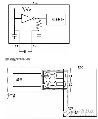
The PC board includes tunable crystals, such as those with RTCs, which do not exclude ultrasound. The crystal may be destroyed by resonance.
Crystal start-up time
The start-up time of the crystal depends to a large extent on the characteristics of the crystal and the circuit layout. High serial equivalent resistance (ESR) and excessive capacitive loading are major factors in extending startup time. Using a crystal with the recommended characteristics and a circuit in accordance with the recommended circuit layout typically starts the crystal in less than a second.
Battery connection
Most FS RTCs include a battery input pin. The battery is used to keep the clock moving normally when the main power is turned off. For most designs, the battery used is a button lithium battery.
Some RTCs use the supply voltage as a reference to determine when VCC is an active level. When VCC is below the minimum, the device enters write protection, disabling external access to the device. When the device is operating under VCC conditions, the VBAT input will be in a high-impedance state. If the battery is not connected to VBAT or is connected to a serial diode, the VBAT input is floating high, causing the RTC to enter write protection. Anti-charge write protection is provided inside most of the FS's clock to eliminate external diodes.
Read/write time and date
Since internal register updates can be made during read or write without data corruption, most FS clocks provide a way to ensure access time and date.
The auxiliary buffer register (secondary buffer) is also used on the serial clock. When accessing (reading) the RTC, the current time and date are transferred to the auxiliary register. A pulse read signal will read data from the auxiliary register and the contents of the auxiliary register will remain unchanged as the internal registers are continuously updated. The next access (when the chip is active, reset or started) will transfer the data again. A similar process occurs when a register is written, unless the data is not flushed by the internal registers prior to access.
The user registers are sealed with TE bits or R and W bits over time keeping the non-volatile (NV) RAM clock.
There are multiple bus clocks. There are several ways to ensure that the time and date registers are unchanged between visits. The following methods are:
Set bit
When the SET bit of the B register is set to 1, the user double buffer time and date registers are latched. The internal registers are still constantly updated.
UIP logo
The update flag bit (UIP) in the process will generate one pulse per second. When the UIP bit goes high, the update will occur after 244uS. If the UIP bit is read low, the user can read the register data for at least 244uS to avoid errors during the update.
UF interrupt
If enabled, an interrupt is generated after each update cycle, which indicates that the valid time and date information can be read for 999ms.
Default register value
If there is no special description in the data sheet, the initial power-on register value is undefined. That is, they are the same as DROM or SRAM: after initial power-up, the actual data used is random.
Discover and solve problems in new designs
Can't communicate with RTC
In the process of new design and problem solving, there are a number of ways to help determine the cause of the problem. For example, if it appears that the device is not communicating at all, it is often worthwhile to determine if the device is not read, written, or both. If the device has software-enabled features, such as a square wave output, trying to make that feature effective is a good way to decide if it can write to the device. On 2-wire devices, the oscilloscope can determine if the clock sends an acknowledgment signal after each byte is transmitted. The following paragraphs describe some of the additional design issues and tips for solving them."
A real-time clock chip with a backup battery switches between VCC and VBAT with a comparator. Some real-time clock chips use the battery voltage as the reference voltage, and the other uses a reference voltage to determine when VCC is active. When VCC drops to the trigger point of the comparator, it cannot be read or written. The prohibition of reading and writing at one voltage helps inadvertently write to the processor, which no longer has a valid supply. Moreover, when the VCC voltage is higher than the trigger point, the comparator switches the internal power supply to VCC to prevent the battery from running out. In a device with a battery voltage reference, a floating battery input, a diode input between the battery and VBAT, or a battery with too high a voltage can stop communication with the RTC. Make sure VBAT is within the valid voltage range and there is no diode between the battery and the battery input pins.
The serial clock requires the correct write of the command byte or slave address to the device. Incorrect commands/addresses often cause the device to ignore read operations. In those cases, the data I/O port terminates in a high impedance state. On a serial line with a pull-up resistor, the data repetition is often 0XFF. In the 3-wire interface, if the I/O port has an internal pull-down resistor, the data is often 0. In other cases, data repetition is often the value of the last bit of the command byte. Some serial clocks are output with separate inputs to allow the processor to coordinate operation at a lower supply voltage. Failure to connect a valid supply to the input will prevent the I/O port from driving high. Finally, if the software cannot switch the processor's port (the input/output pin to the clock) from the output (write command section) to the input (read data), the output data may be all 0s or all ones.
Invalid time and data value
Most time and date registers can accept any value, including invalid values. If an invalid value enters the register, the value will continue to increase until it matches the bit that was flipped, reaching a minimum. If the clock is in the wrong mode. It may also result in invalid values, for example, binary code instead of BCD code, or 12-hour system instead of 24-hour clock.
Data loss/data corruption
There are two situations that can cause data loss: an inadvertent write clock or an inverted glitch pulse voltage is applied to the IC. Because the CH or /EOSC bits (on the clock with the crystal control bit) are in the default stop state, the data loss caused by the inverting voltage input to the IC is sometimes identifiable. In addition, most, but not all, of the data in the registers will be corrupted. Inadvertent writes typically occur during the power cycle, but usually only affect one register without affecting the serial clock.
Many modern switching power supplies will generate a -5V or -6V or even larger glitch on the VCC during power up and/or power down. This negative voltage is coupled to the internal clock supply via an input protection diode. If the power supply can supply more current than the battery, the data will be lost. In some cases, this negative glitch voltage can be clamped with a Schottky diode. The negative voltage source on the other clock comes from the RS232 connector. If the PCB with the clock chip is powered down, the powered PC or other device is connected to that board via the RS232 connector, and the RS232 transceiver chip may pass the negative voltage to other chips on the unpowered PCB.
Inadvertent writing can also cause data corruption. The processor can write erroneous data during power-up or power-down before write protection is active. At power-up and power-down, the interface circuitry may force the input pins into a write state. In the case of a multi-bus clock, the address signal is latched on the falling edge of ALE. If /WE and /CS become low voltage before the device is write protected, the last accessed data in the last register will be corrupted. The rise and fall times of the VCC should be checked for error in the data sheet.
Incorrect interrupt program processing causes intermittent data problems. In some cases, time and data information is copied to RAM, and replication is not synchronous. Finally, improper circuit configuration (IEC) hardware can cause strange behavior.
Crystal problem
The most common reason why time cannot be increased is that the crystal is not enabled. Many FS clock chips have a control bit (usually located in the second register) that must be set before the crystal is active.
To extend battery life, the oscillator circuit is designed for low power consumption. Crystal connection problems can reduce the closed-loop gain and prevent the crystal from working. The external capacitor connected to the crystal also reduces the closed-loop gain, increasing the start-up time or preventing vibration. The oscilloscope's probe also blocks vibration. A crystal with an equivalent series resistance (ESR) of 45K or more will also reduce the closed-loop gain. Finally, the solder cleaner left on the board may prevent the crystal from starting.
LCD Tonch Screen For Iphone 11
Lcd Tonch Screen For Iphone 11,Lcd Touch Screen For Iphone X11Promax,Lcd Display For Iphone X11Promax,Mobile Lcd For Iphone X11Promax
Shenzhen Xiangying touch photoelectric co., ltd. , https://www.starstp.com