FPGA is a programmable chip, so FPGA design methods include hardware design and software design. The hardware includes FPGA chip circuit, memory, input and output interface circuits and other devices. The software is the corresponding HDL program and the most popular embedded C program. Hardware design is the foundation, but its method is relatively fixed. This book will introduce it in detail in section 4. This section mainly introduces the design method of software.
At present, the microelectronics technology has developed into the SOC stage, that is, the integrated system stage, which has a revolutionary change with respect to the design idea of ​​the integrated circuit (IC). The SOC is a complex system that integrates the functions of a complete product on a single chip, including core processors, memory units, hardware acceleration units, and numerous external device interfaces. It has characteristics such as long design cycle and high implementation cost. The design method must be a top-down software-hardware co-design from the system level to the functional module, and achieve a seamless combination of software and hardware.
Such a huge amount of work is obviously beyond the capabilities of a single engineer, so it needs to be implemented according to a hierarchical and structured design method. First, the chief designer divides the entire software development task into several operational modules, evaluates its interfaces and resources, and formulates corresponding behavioral or structural models, which are then assigned to designers of the next level. This allows multiple designers to design different modules in a hardware system at the same time and be responsible for the modules they design; then the upper-level designer performs functional verification on the lower modules.
The top-down design flow begins with a system-level design and is divided into a number of second-level units. Each secondary unit is then divided into the next-level basic unit and continues until it can be directly implemented using basic modules or IP cores. So far, as shown in Figure 1-6. Popular FPGA development tools provide hierarchical management that can effectively sort through intricate layers and easily view the source code of a certain level of modules to correct errors.
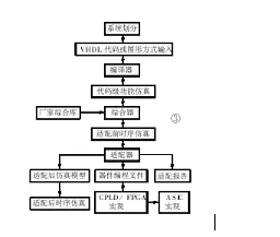
Figure 1-6 top-down FPGA design and development process
In engineering practice, there is still a problem of software compilation time. Because large-scale designs contain multiple complex functional modules, their timing convergence and simulation verification are very complex. In order to meet the requirements of timing indicators, it is often necessary to repeatedly modify the source files, and then recompile the modified new version until the requirements are met. until. There are two problems here: First, the software compiles takes as long as hours or even weeks, which is unacceptable for development; secondly, the results of recompilation and placement and routing are very different and will meet the timing Circuit damage. Therefore, it is necessary to propose a software tool that can effectively improve the design performance, inherit the existing results, and facilitate the team-based design. FPGA vendors are aware of this type of demand and have developed corresponding software tools for logical locking and incremental design. For example, Xilinx's solution is PlanAhead.
Planahead allows high-level designers to partition the corresponding FPGA chip area for different modules, and allows the underlying designer to independently design, implement, and optimize within a given area, and then integrate the design after each module is correct. If there is an error in the design integration, you can modify it alone without affecting other modules. Planahead combines the structural design method, the team-based cooperative design method, and the reuse inherited design method. It effectively improves the design efficiency and shortens the design cycle.
However, as can be seen from its description, the new design method has high requirements for the system top designers. In the initial stage of design, they not only need to evaluate the resources consumed by each sub-module, but also need to provide the corresponding timing relationship; In the latter part of the design, it is necessary to complete the corresponding revision according to the implementation of the underlying module.
Typical FPGA Development ProcessThe FPGA design flow is the process of developing the FPGA chip using EDA development software and programming tools. FPGA development process is generally shown in Figure 1-7, including the main steps of circuit design, design input, functional simulation, comprehensive optimization, post-synthesis simulation, implementation, post-wiring simulation, board-level simulation, and chip programming and debugging.
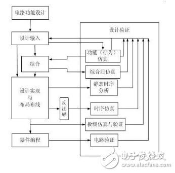
Figure 1-7 General flow of FPGA development
Circuit design
Before the system design, the first thing to do is plan preparation, system design and FPGA chip selection. According to the task requirements, such as the index and complexity of the system, the system engineer weighs the working speed and various resources and costs of the chip itself, and selects a reasonable design scheme and a suitable device type. In general, a top-down design method is used to divide the system into a number of basic units, and then each basic unit is divided into basic units of the next level. This is done until the EDA component library can be directly used.
Design input
Design input is the process of expressing the designed system or circuit in a form of development software requirements and inputting it to EDA tools. Commonly used methods include hardware description language (HDL) and schematic input methods. Schematic input mode is the most direct way of description. It is widely used in the early stage of programmable chip development. It pulls out the required devices from the component library and draws schematics. Although this method is intuitive and easy to simulate, it is inefficient and difficult to maintain, which is detrimental to module construction and reuse. The main drawback is the poor portability. When the chip is upgraded, all the schematics need to be changed. At present, the most widely used in actual development is the HDL language input method. Using text description design, it can be divided into ordinary HDL and behavioral HDL. Common HDLs include ABEL, CUR, etc., and support expressions such as logic equations, truth tables, and state machines, and are mainly used for simple, small designs. In medium-to-large-scale projects, behavioral HDL is mainly used. Its main languages ​​are Verilog HDL and VHDL. Both of these languages ​​are the standards of the Institute of Electrical and Electronics Engineers (IEEE). The common features of the two languages ​​are: language is independent of the chip technology, facilitates top-down design, facilitates the partitioning and transplantation of modules, and has good portability. Has a strong logic description and simulation capabilities, and the input efficiency is high.
3. Functional simulation
Functional simulation, also known as pre-simulation, is to verify the logic function of the circuit designed by the user before compiling. At this time, the simulation has no delay information, and only the preliminary function is detected. Before the simulation, first use the waveform editor and HDL to create waveform files and test vectors (that is, combine the input signals of interest into a sequence). The simulation results will generate report files and output signal waveforms, from which you can observe the signal of each node. Variety. If an error is found, the design modification logic design is returned. Commonly used tools include ModelSim from Model Tech, VCS from Sysnopsys, and NC-Verilog and NC-VHDL from Cadence.
4. Comprehensive optimization
The so-called synthesis is to translate the description of a higher level of abstraction into a lower level of description. Comprehensive optimization optimizes the generated logical connections according to goals and requirements, enabling the hierarchical design to be flat and implemented by the FPGA layout and cabling software. At the current level, synthetic synthesis refers to the process of compiling design input into logical connected netlists consisting of basic logic elements such as AND gates, OR gates, NOT gates, RAM, and flip-flops. It is not a true gate level. Circuit. The actual and specific gate-level circuit needs to use the FPGA manufacturer's layout and routing functions to generate the standard gate-level structure netlist generated after synthesis. In order to be able to convert to a standard gate-level netlist, the HDL program must be written in the style required by a particular synthesizer. Since the synthesis of gate-level and RTL-level HDL programs is a mature technology, all synthesizers can support this level of integration. Common synthesis tools include Synplify's Synplify/Synplify Pro software and comprehensive development tools from various FPGA manufacturers.
5. Post-synthesis simulation
After the comprehensive simulation check whether the integrated results are consistent with the original design. In the simulation, the comprehensively generated standard delay file is back-annotated into the comprehensive simulation model to estimate the impact of the gate delay. However, this step can not estimate the line delay, so there is a certain gap between the actual situation after the wiring, and it is not very accurate. The current synthesis tool is relatively mature, and this step can be omitted for general design. However, if the circuit structure and design intent are found to be inconsistent after layout and wiring, it is necessary to trace back to post-synthesis simulation to confirm the problem. Software tools introduced in functional simulation generally support post-synthesis simulation.
6. Implementation and Place and Route
The implementation is to configure the synthetically generated logic netlist to a specific FPGA chip, and layout and wiring are the most important ones. The layout rationally configures the hardware primitives and the underlying elements in the logic netlist to the inherent hardware structure within the chip, and often requires a choice between speed optimization and area optimization. According to the topological structure of the layout, the wiring utilizes various connection resources within the chip to properly and accurately connect the components. At present, the structure of the FPGA is very complex, especially when there are timing constraints, it is necessary to use a timing-driven engine for placement and routing. After the wiring is completed, the software tool will automatically generate a report that provides information on the use of various parts of the design. Since only FPGA chip manufacturers know the structure of the chip best, place and route must choose the tool that the chip developer offers.
7. Implementation and Place and Route
Timing simulation, also known as post-simulation, refers to the back-tagging of placement and routing delay information to the design netlist to detect timing violations (ie, not meeting timing constraints or inherent device timing rules, such as settling time, maintaining Time, etc.) Phenomenon. Timing simulation contains the most complete and accurate delay information, which can reflect the actual work of the chip. Because different internal delays of different chips are different, different layout and routing solutions also have different effects on the delay. Therefore, after placement and routing, it is necessary to perform timing simulation on the system and each module, analyze its timing relationship, estimate system performance, and check and eliminate competitive risks. Software tools introduced in functional simulation generally support post-synthesis simulation.
8. Board Level Simulation and Verification
Board-level simulation is mainly used in the design of high-speed circuits. It analyzes the characteristics of high-speed system such as signal integrity and electromagnetic interference, and is generally simulated and verified by third-party tools.
9. Chip programming and debugging
The final step in the design is chip programming and debugging. Chip programming refers to generating data files (bitstream files, Bitstream GeneraTIon) that are used, and then downloading programming data to the FPGA chip. Among them, the chip programming needs to meet certain conditions, such as programming voltage, programming timing and programming algorithms. Logic Analyzer (LA) is the main debugging tool for FPGA design, but it requires a large number of test pins, and LA is expensive. Currently, mainstream FPGA chip manufacturers provide embedded on-line logic analyzers (such as ChipScope in Xilinx ISE, SignalTapII in Altera QuartusII, and SignalProb) to solve these problems. They only need to occupy a small amount of logic resources of the chip. High practical value.
When people search gaming laptop, indicates that they need high performance 15 Inch Gaming Laptop, comes with big screen size, high cpu, large memory and storage, high resolution display, quality bigger 12000mAh battery, 2MP Camera, etc. 15 or 14 inch 500 Dollar Gaming Laptop, 10th generation laptop, 11th gen gaming laptop, 12th generation laptop, Laptop Intel Core I7, Intel I5 Laptop are the Top 10 Gaming Laptops. Every gamer want to buy Gaming Laptop with higher processors, big 8GB, 12GB, 16GB system memory ram, large Solid State Drive so that can handle or storage digital data at a high speed, 1920*1080 Full HD Slimmer screen provides user stunning vivid visuals, fingerprint reader, backlight keyboard, etc.
Nowadays 11th Laptop is the most competitive cpu, cause performance is better than 10th, but price is nearly same; besides, Solid State Drive cost 512GB is the most welcome and competitive one.
Of course, You can also contact us directly and share your exact requirements, so that we can send the right and valuable information quickly.
Gaming Laptop,Top 10 Gaming Laptops,500 Dollar Gaming Laptop,15 Inch Gaming Laptop,Buy Gaming Laptop
Henan Shuyi Electronics Co., Ltd. , https://www.shuyilaptop.com