Prof. Zhou Ligong's new book "Programming for AMetal Frameworks and Interfaces (Part 1)" introduces the AMetal framework in detail. By reading this book, you can learn highly multiplexed software design principles and development ideas for interface programming. Focus on your own "core domain", change your own programming thinking, and achieve common progress between the company and the individual. Authorized by Professor Zhou Ligong, from now on, the Zhiyuan Electronic Public Number will serialize the contents of the book, and is willing to share it.
The second chapter is the ADC signal conditioning circuit design . This article is 2.3 necessary measures, 2.4 actual test verification and 2.5 application description .
2.3 necessary measures
A complete acquisition circuit block diagram is shown in Figure 2.19. From the sensor or signal source to the final ADC data output, the signal conditioning process such as input range adjustment and multi-channel multiplexing is required. In addition to the ADC itself, the design of the entire acquisition channel link needs to be considered in order to achieve good acquisition accuracy.

Figure 2.19 Typical acquisition circuit block diagram
The issues to consider when designing the acquisition channel are:
The size of the signal and the range of the ADC full-scale input.
The polarity of the signal and the polarity of the ADC input.
The number of channels of the signal, do you need multi-channel simultaneous sampling, or use a multiplexed input?
Is the signal a single-ended input or a differential input?
> > > 2.3.1 Input range matching
Sensor signals tend to be very weak and the amplitude may only be a fraction of the ADC range. Matching the amplitude of the maximum input signal to the ADC range is important for maximum ADC conversion accuracy. Assuming that the signal to be converted varies between 0V and 2V, and VREF is equal to 3V, the ADC conversion value of the maximum signal is 2729 (2.0V), as shown in Figure 2.20. Thus, there are 1366 unused conversion values, ie the accuracy of the converted signal is lost.
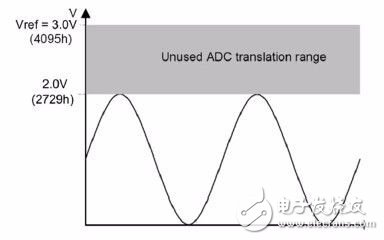
Figure 2.20 Input Signal Amplitude and ADC Measurement Range
It is best to use an external preamplifier that converts the range of the input signal to the range of the ADC module. For example, using the LMV358A to build a 10x non-inverting amplifier, the 0~300mV input signal is converted to 0~3V.
It is also possible to use an external amplifier to build the superposition circuit, complete the bipolar positive and negative input, convert to a unipolar input, and build an instrumentation amplifier to convert the differential input into a single-ended input.
> > > 2.3.2 Multi-channel sampling setup
When considering hardware costs, it is common practice to multiplex one ADC with multiple acquisition channels. The LPC82x has 12 analog input pins, and the chip has a multiplexed structure inside, as shown in Figure 2.21.

Figure 2.21 Multiplexed Equivalent Circuit of LPC82x Analog Input Channel
When using this time division multiplexing structure, it is very easy to cause a drop in accuracy by the following two problems:
Excessive signal source impedance of the channel results in insufficient setup time and a reduced voltage value.
The channel switching time is too fast, and the parasitic capacitance of the common side of the multiplexer causes crosstalk of signals on adjacent channels.
Although the influence of signal source impedance has been designed to completely solve the buffer op amp, considering the cost factor, it is sometimes unacceptable to add an op amp to each channel. A more reasonable configuration is to use an op amp on a signal channel with high amplitude accuracy requirements. The signal source on the less demanding channel is directly input to the ADC channel.
This hybrid configuration requires two considerations: the direct input channel is a high speed signal and requires high bandwidth, or is a low speed signal and requires bandwidth limiting. When the direct input channel is a high-speed signal reference circuit, see Figure 2.22. In order to avoid voltage residual caused by channel crosstalk, the capacitor cannot be connected in parallel. The key to the design is that the signal source impedance matches the sampling rate.

Figure 2.22 Multi-channel sampling circuit when the direct input channel is a high-speed signal
The limit value of the source impedance of the direct input channel is quantized according to the sampling rate. For ease of calculation, take a single LPC82x analog input channel in the multiplexed structure. See Figure 2.23 for the equivalent circuit.
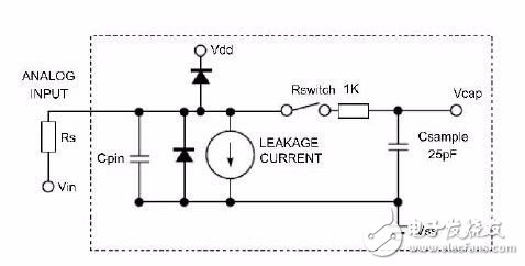
Figure 2.23 LPC82x equivalent circuit of a single analog input channel
From left to right, R S is the external source impedance, C PIN is the input pin capacitance (substantially negligible), R SWITCH is the multiplexed switch resistance + sampling switch on resistance, and C SAMPLE is the sampling capacitor. The switch is closed during sampling, R S , R SWITCH , C SAMPLE constitute a single-pole RC network, and its time constant can be expressed as:

Assume that at the beginning of sampling, the voltage on the sampling capacitor is zero, and the relationship between the voltage on the capacitor and the rise time can be expressed as:

It can be seen that the voltage on the sampling capacitor can be determined as a percentage of the input signal voltage value according to the change time. Assuming R S is 0, when the voltage on the sampling capacitor is 99.32% of the input voltage value, there will be 0.68% (the remaining percentage) of the voltage can not be accurately obtained, that is, the minimum resolution is 0.68%, which is 7.2 bit The resolution of the ADC is the same. The conversion formula for the remaining percentage and ADC digits is log 2 (1/percentage percentage) log2 (1/percentage percentage), and the typical conversion results are shown in Table 2.4.
Table 2.4 Setup Time and ADC Accuracy

According to the calculations in this table, if the ADC can not give enough sampling time, the accuracy of the ADC will be reduced. Assuming a 12-bit ADC with a sampling rate of 1 Msps, the effective sampling time is 750 ns. When R S is 0, 750ns>200ns, the sampling capacitor can achieve much higher accuracy than 12 bits, and the sampling time is sufficient. If you now add 5KΩ internal resistance to the signal source, you can get: If you want to achieve 13bits accuracy, the ADC needs at least 1350ns sampling time:

The sampling time of 750ns is not enough. At this point, you can change the sampling rate of the ADC by changing the software to get longer sampling time. To determine whether the sampling rate should be reduced, the highest source impedance allowed is the reference value at the LPC82x maximum sampling rate of 1 Msps. Consider the signal establishment to 1/2LSB, the calculation process is as follows:

This limit value indicates that the multi-channel sampling circuit using the direct input channel of Figure 2.22 as a high-speed signal, the highest signal source impedance should not exceed 2kΩ, otherwise the sampling rate needs to be reduced.
When the reference circuit of the direct input channel is a low-speed signal, see Figure 2.24, there is no requirement for the source impedance, but the adjacent input channels on both sides of the channel need to be grounded. To summarize the multi-channel sampling setting method, see Table 2.5. The high-speed signal refers to the signal that needs to be sampled by the waveform, such as the waveform of the acquisition network. The low-speed signal refers to a signal that only focuses on the DC component, such as the power supply voltage and the output voltage of the temperature sensor.

Figure 2.24 Multi-channel sampling circuit when the direct input channel is a low-speed signal
Table 2.5 Selection method of multi-channel sampling circuit

> > > 2.3.3 Power Distribution Strategy
Power supply noise is an important source of noise on the board. In order to reduce interference, it is recommended that the analog and digital sections be powered independently using a voltage regulator, as shown in Figure 2.25.
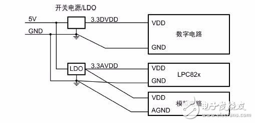
Figure 2.25 The analog part and the digital part are independently powered
> > > 2.3.4 PCB layout processing
The switching noise of digital signals is another major source of interference on the board. To avoid interference with digital circuits on the board that interfere with analog circuits, the following rules should be followed:
Analog part and digital parts are placed in sub-areas to avoid cross placement, as shown in Figure 2.26.

Figure 2.26 Analog and Digital Devices Subregional Placement
Divide the ground plane, and then connect the analog ground plane to the digital ground plane at a single point to avoid interference introduced through the common ground loop, as shown in Figure 2.27.

Figure 2.27 Split ground plane in a single point connection
Analog traces and digital traces are avoided to avoid parallel traces. If it is unavoidable, add ground traces to simulate traces. See Figure 2.28 for details.

Figure 2.28 Avoiding Digital Traces Interfering with Analog Traces
2.4 Measured verification
In order to verify the effectiveness of the improvement method, an actual circuit board was produced. Test the key accuracy specifications of the LPC824 internal ADC and compare it with the test data of the finished development board AM824. The main test data is noiseless resolution, INL, offset error, and gain error.
> > > 2.4.1 Noise-free resolution
Noise-free resolution is defined as the ADC circuit measuring a noise-free, stable DC voltage source, counting multiple consecutive samples of data, and outputting digital codes to maintain a non-bounced number of bits. The noise-free voltage source uses a dry battery. Ideally, the output code does not jump and there is only one output code.
On the original AM824 development board, repeat a test of 200 dry batteries, the data histogram obtained is shown in Figure 2.29.

Figure 2.29 AM824 development board test DC signal code distribution
Repeat the test of the same dry battery 200 times on the board using the improvement measures in this paper. The data histogram obtained is shown in Figure 2.30.

Figure 2.30 Code distribution of standardized circuit board test DC signals
After comparison, it is found that the original data beats at 6 digits and is converted to a resolution of 3 bits, which means that if the original development board is used, the resolution of 9-bit resolution can be utilized at most. But on the new board, we see that the data is relatively concentrated and the jitter is only 3 bits, the measurement accuracy is higher, and the 10-bit resolution accuracy can be used.
> > > 2.4.2 Integral Nonlinearity (INL)
INL is an important parameter that characterizes the accuracy of the ADC. In the full range of the ADC, set the input voltage value from small to large, and sequentially collect a series of data points at equal intervals, which can linearly fit a line closest to these data points. Ideally, the ADC is linear and the acquired data points should all fall on that line. The degree of deviation of the actual sampled data point from the fitted line characterizes the nonlinearity of the ADC. The data tested on the original AM824 development board is shown in Table 2.6 (Vref=2.5V).
Table 2.6 INL test data of the AM824 development board

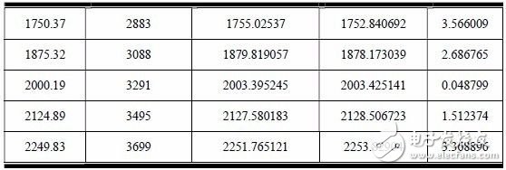
The fitting curve of the INL data of the AM824 development board is shown in Figure 2.31.

Figure 2.31 Fit curve of INL data for AM824 development board
On the board using the improvement measures in this paper, the test data obtained by repeating the test is shown in Table 2.7 (Vref=3V).
Table 2.7 INL test data for standardized boards
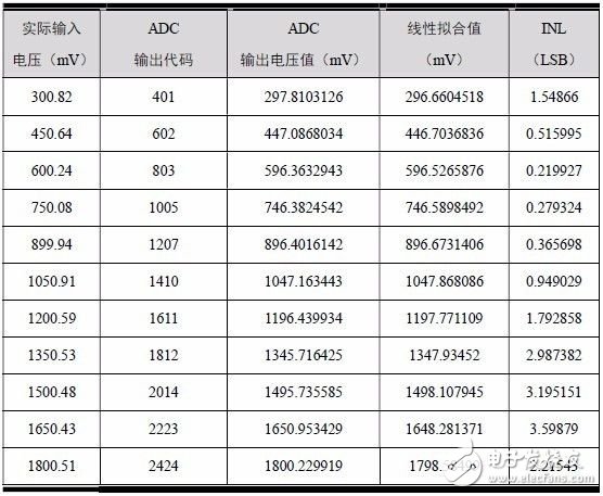
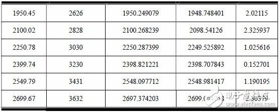
The fitted curve of the standardized circuit board INL data is shown in Figure 2.32.
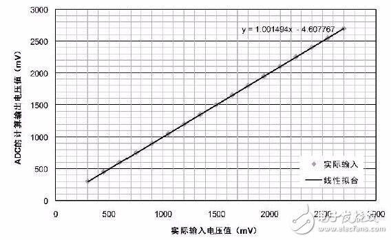
Figure 2.32 Fit curve of standardized circuit board INL data
By comparing Tables 2.6 and Table 2.7, it was found that after adding these measures to the board, the INL was improved from the original 5.3 LSBs to the later 3.6 LSBs.
> > > 2.4.3 Offset and Gain Error
Offset error
The offset error is defined as the deviation between the first actual transition to the first ideal transition. Ideally, the first conversion should occur when the input signal is 0.5 LSB. The offset error is marked with EO and the test process is as follows:
Adjust the adjustable resistor to produce a continuously variable mV level voltage value input to the normalized board. Observe that the ADC output code becomes 1 with a voltage value of 2.44mV. The reference voltage on the measured circuit board is: 3047.56mV, which is calculated as 1LSB = 3047.56 / (4096 * 2) = 0.74mV.

2. Gain error
Gain error is defined as the deviation between the last actual conversion and the last ideal conversion. Ideally, a conversion from 0xFFE to 0xFFF occurs when the analog input voltage is equal to VREF-0.5LSB. The gain error is marked with EG. The test procedure is: adjust the adjustable resistor to generate a continuously variable voltage value near Vref and input it to the normalized circuit board. Observe that the ADC output code becomes 0xFFF and the voltage value is: 3046.35mV.

2.5 Application Notes
Summarize the improved precision board test results of the standardized circuit board and AM824 development board as shown in Table 2.8.
Table 2.8 ADC Test Accuracy of Standardized Circuit Board and AM824 Development Board

The data in the table shows that after the improvement of the method mentioned above, in addition to the slight increase in the offset voltage caused by the increase in the ADC-driven op amp, all parameter specifications can be further improved. The noise-free resolution in the AM824 development board is relatively low, according to the formula log 2 (1/bounce LSB) log2 (1/bounce LSB), around 9 bits. INL is also 9 bits according to the formula log 2 (1/error LSB) log2 (1/error LSB).
With an improved design of the standardized board, the on-chip ADC can perform better performance, with noise-free resolution and INL performance up to 10 bits, suitable for applications with an accuracy rating of 0.5%.
In practical applications, if the user needs to modify parameters such as filter bandwidth or input range, it can be done in the following aspects, only need to make some adjustments on parameters or channel circuits, as shown in Table 2.9.
Table 2.9 User Parameter Selection

Glass Plate Type Liquid Level Gauge Self-closing Valve Body
Glass plate type liquid level gauge self-closing valve body,liquid level gauge self-closing valve body,self-closing valve body,liquid level gauge self-closing valve body price
Taizhou Jiabo Instrument Technology Co., Ltd. , https://www.taizhoujbcbyq.com