Xilinx's Virtex UltraScale family of devices are implemented in a 20nm process with high performance, high serial I/O bandwidth and powerful logic, making it the industry's only high-end FPGA in the 20nm processor. Achieve up to 400G network design applications and large-scale ASCI prototyping and simulation.
The Xilinx Zynq®-7000 All Programmable SoC (AP SoC) family integrates ARM processor core-based software programming applications with an FPGA-based hardware programming application that enables hardware accelerators for analysis and on a single device. CPU, DSP, ASSP or some signal processing modules are integrated. In this series, single-core Zynq-7000 and dual-core Zynq-7000 devices are included. The key point is that the Zynq-7000 series applies the power consumption of the chip to the extreme, and can enhance the fully scalable SoC platform for users' own applications.
Aldec HES-US-440
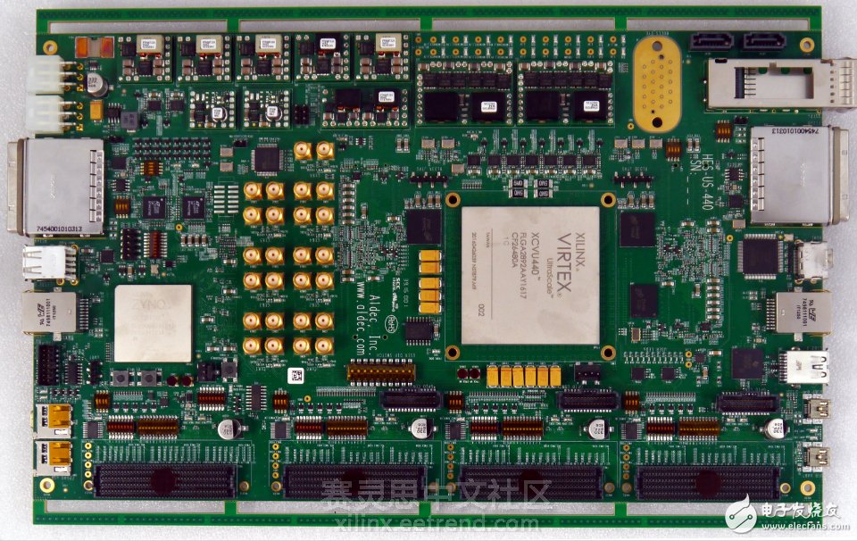
Recently, Aldec has released the latest FPGA-based HES prototype prototype, the HES-US-440, which has logic capabilities of up to 26 million ASIC gates. In addition, the board is based on the Xilinx Virtex UltraScale VU440 FPGA and integrates a Xilinx Zynq Z-7100 SoC chip that not only acts as a peripheral for the board but also provides a host interface on the board. In Aldec's board release, Aldec's HES-DVM software/hardware verification platform was also released. On this platform, not only simulation acceleration but also user-defined customization besides the board's own physical prototype can be verified. Module. In addition, users can apply this prototyping board directly to HPC (High Performance Computing) applications. This board is shown below:

Figure 1: Aldec HES-US-440 Prototyping board
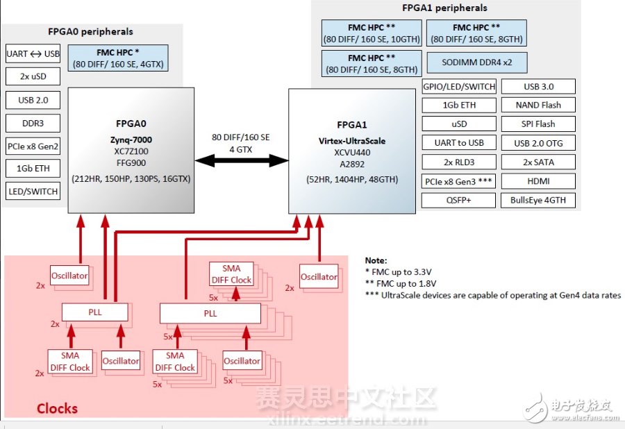
Aldec's HES-US-440 board has a rich and extensible external interface that makes it easy to implement your own designs, such as FMC HPC connections, including PCIe, USB3.0 and USB2.0 OTG, UART/ USB bridge, QSFP+, Ethernet interface up to 1Gbps+, HDMI interface, SATA interface, etc. In addition, NAND and SPI flash memory units are integrated on the board, as well as two micro SD card slots. The figure below is the structure diagram of the board:

Figure 2: Aldec HES-US-440 board structure
As can be seen from the above figure, the structure of the entire HES-US-440 board is similar to the internal structure of Zynq. It integrates two ARM dual-core Cortex-A9 CPUs. This board integrates two different series of Xilinx FPGAs, one Virtex. UltraScale XCVU440 is a Zynq-7000host module that can be connected independently between two chips. Therefore, Xilinx will undoubtedly bring great scalability and flexibility to users.
in conclusion:Alec's HES-US-440 is not the only development board for Aldec's application of Xilinx's FPGA board. On the contrary, many of Aldec's application boards are based on Xilinx's FPGA chips. The reason why Aldec chose Xilinx's FPGA boards is undoubtedly because these FPGAs can provide users with higher performance utilization at the same cost, such as Zynq 7000 series, such as Virtex UltraScale series, etc. I believe Xilinx will be in the future. Develop more powerful FPGAs that attract partners.
The wire harness simplifies the building of these larger components by integrating the wiring into a single unit, or several units, for [drop-in" installation. By binding the many wires, cables, and subassemblies into a harness, the OEM or installer only has one component to install. In addition, a wire harness allows the completed assembly to be better secured against the effects of abrasion and vibration, and by constricting the wires into a non-flexing bundle, usage of space is optimized.
Game Machine Wire Assembly, wire harness for gaming machine, electrical wire assembly, gaming wire harnesses
ETOP WIREHARNESS LIMITED , https://www.wireharnessetop.com