Text /EIJI FUKAWA, Cypress Semiconductor
Wireless sensor nodes reduce implementation costs by reducing sensor size, simplifying maintenance issues, and extending battery life. In fact, if you focus on a battery-free design, you will be able to achieve greater cost-effectiveness.
The best way to design a batteryless device is to reduce the average power consumption of the wireless sensor system through technologies such as Bluetooth Low Energy (BLE) for communication and energy harvesting.
Figure 1 is an architectural diagram of a miniature wireless sensor. The sensor is created using a microcontroller (MCU) with integrated BLE radio that can be fully powered by the power supply provided by the energy harvesting power management integrated circuit (IC).
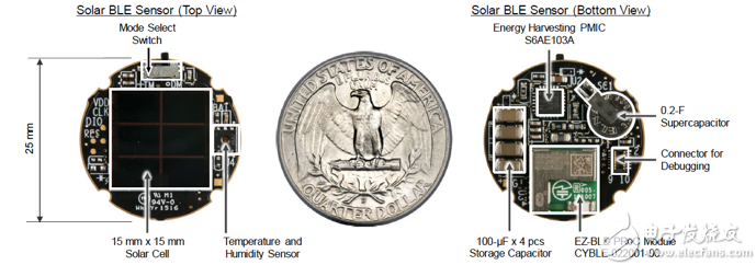
[Figure 1 | The miniature wireless sensor was created using a microcontroller (MCU) with integrated BLE radio, optimized to operate with only the power supply provided by the energy harvesting power management IC. The picture shows the complete wireless sensor -- the CYALKIT-E02 solar powered BLE sensor reference design kit (RDK). ]
BLE optimization
In order to operate only with the power supply provided by the energy harvesting IC, the sensor must optimize its BLE system to reduce power consumption. First, the designer must understand the details of the BLE subsystem. Next, you need to write firmware code to meet the requirements of each run/power mode. The designer must then analyze the actual power consumption to confirm the various assumptions to further improve the system's energy efficiency.
A description of the power reduction technology can be found in the Cypress CYALKIT-E02 Solar Powered BLE Sensor Reference Design Kit (RDK). The RDK includes a Cypress PSoC 4 BLE and S6AE10xA Energy Harvesting Power Management IC (PMIC).
A simple, power-optimized BLE design first configures the BLE radio to be a beacon in a non-connectable broadcast mode. A BLE beacon is a one-way communication method that broadcasts at regular intervals. It contains some smaller packets (30 bytes) that are sent out as a broadcast packet. Beacons are found to be able to push messages, app actions and tips on a variety of smartphone or computer applications.
Figure 2 shows the BLE link layer format for the broadcast channel packet format. The BLE link layer has "Preamble", "Access Address", "Protocol Data Unit (PDU)" and "Cyclic Redundancy Code (CRC)" (Cyclic Redundancy Code) ). Please note that the following information applies only to the broadcast channel packet format and does not include a Data Channel Packet.
"Preamble" must be set to "10101010b"
"Access Address" must be set to "10001110100010011011111011010110b (0x8E89BED6)"
"PDU" contains "header" and "net payload"
The packet structure of the BLE beacon belongs to "broadcast data" in "net payload".
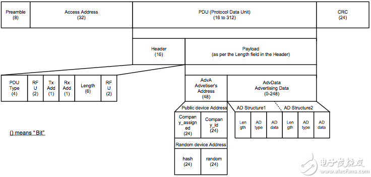
[Figure 2 | BLE Link Layer Format for Broadcast Channel Packet Format]

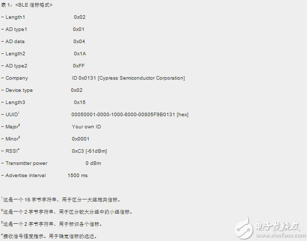
[Figure 3 | BLE Beacon Packet Format]
Table 1 lists the settings.
The average current consumption can be calculated using the voltage and current waveforms to determine the efficiency of the BLE design. Figure 4 shows the power consumption results for a powerless optimized design.
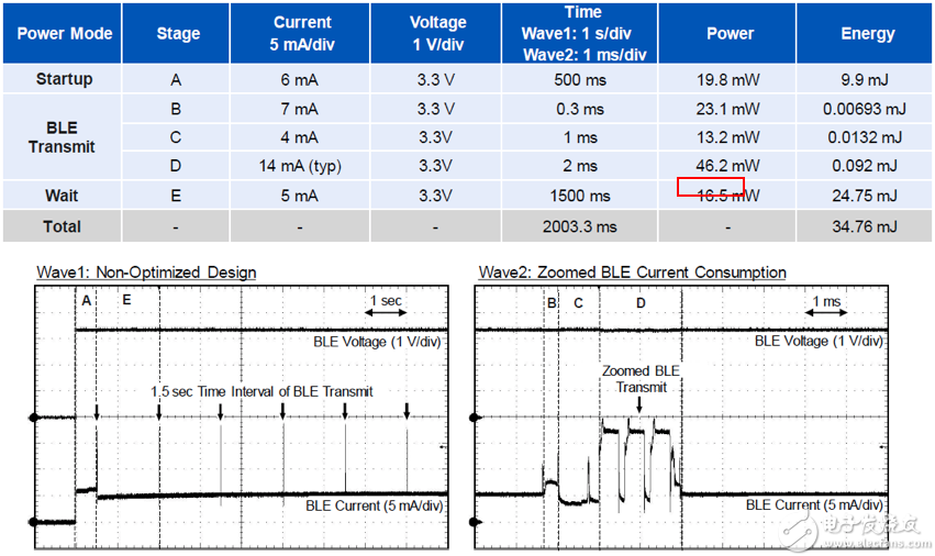
[Figure 4 | Current consumption of BLE design without power optimization]
The average current is approximately 5 mA and the total power consumption from startup to standby is 34.76 mJ. In order to operate with ambient energy, we need to reduce the current consumption.
Low power consumption by optimizing firmware
Reduce the average current consumption of the BLE design by optimizing the following four features:
Low power start
2. Deep sleep
3. IMO clock settings
4. Debugging options
When the system is in low power mode, the watchdog timer (WDT) needs to be used to wake up the system.
Low power start
After a power-on reset (POR), the BLE system initializes these components by calling the startup functions of the different components. Perform low-power operation by performing the following steps during initialization:
1. Turn off the 24-MHz external crystal oscillator (ECO) to reduce power consumption when the 32.768-kHz watch crystal oscillator (WCO) is started.
2. After 500 ms (WCO boot time), enable WDT to wake up the system.
3. Configure the MCU to be in deep sleep mode during the 500 ms WCO boot time.
4. Once the WCO is enabled, restart the ECO to enable the BLE subsystem (BLESS) interface.
5. Place the WCO in low power mode and change the low frequency clock (LFCLK) source from the 32-kHz internal low speed oscillator (ILO) to WCO.
6. Enable WDT to wake up the system.
7. Place the MCU in deep sleep mode.
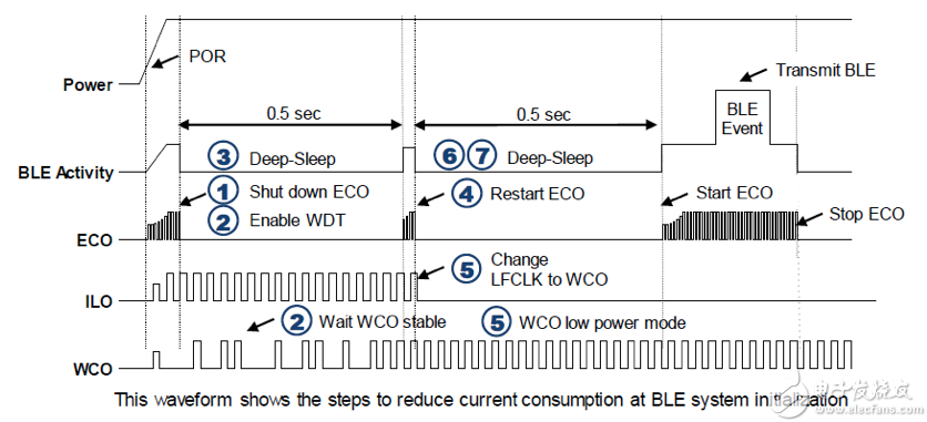
[Figure 5 | Low Power Startup Waveform]
Deep sleeping
The user design should manage the system clock, system power mode, and BLESS power mode to achieve low power operation of the BLE MCU.
During the BLE event interval, it is recommended to implement deep sleep by performing the following steps:
1. Turn off the ECO to reduce power consumption.
2. After 1.5s (BLE event interval), enable WDT to wake up the system.
3. Place the MCU in deep sleep mode.
4. After 1.5s, restart the ECO to enable the BLE subsystem (BLESS) interface.
5. Send BLE broadcast data.
6. Repeat from step 1.
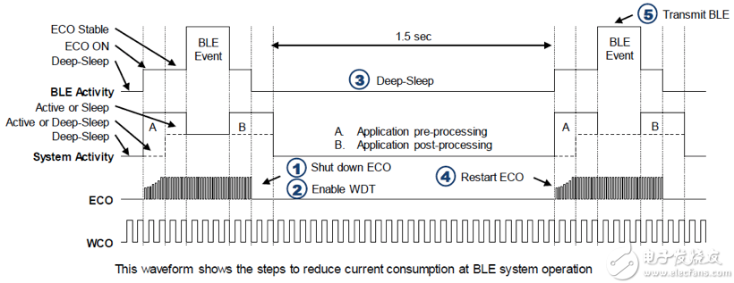
[Figure 6 | Deep Sleep Waveform]
IMO clock setting
The 3-MHz to 48-MHz internal main oscillator (IMO) is the primary internal clock source. The IMO's default frequency is 48 MHz and can be adjusted in 1 MHz steps from 3 MHz to 48 MHz. At the default calibration settings, the tolerance of the IMO to the RDK in this example is ±2%. Figure 7 shows an example of total power consumption after changing the IMO frequency.

[Figure 7 | IMO DC Specifications and Example Total Power Consumption]
Debug selection
The Serial Wire Debug (SWD) pin is used for runtime firmware debugging during development. Configuring the SWD pin to debug mode increases current consumption. Therefore, these pins should be switched to General-Purpose Input and Output (GPIO) mode at the final version to allow them to be used for device programming during a chip reset.
We can use the voltage and current waveforms to calculate the average current consumption of the BLE design to confirm the design optimization. Figure 8 shows the power consumption results for a power optimized design.
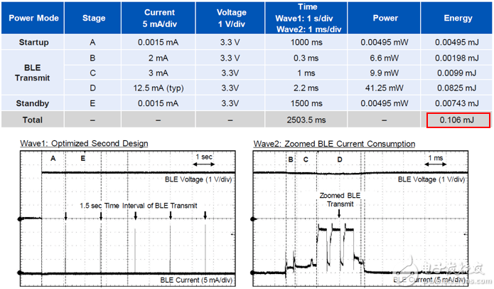
[Figure 8 | Current Consumption of Power Optimized BLE Design]
The average current is approximately 1.5 μA and the total power dissipation from startup to standby is 0.106 mJ.
Run with energy harvesting technology
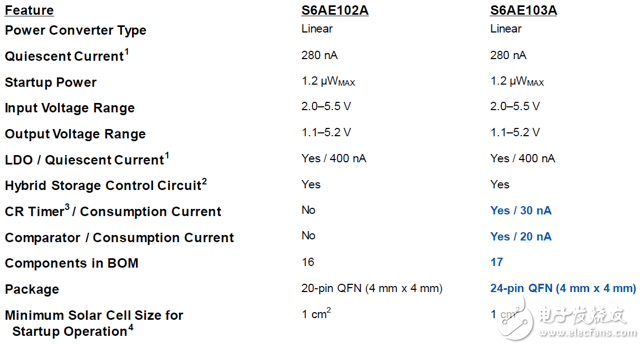
At this average current and total power consumption level, it is necessary to confirm that the system can operate with energy harvesting technology. Figure 9 shows a block diagram of an energy harvesting system. The system uses the S6AE10xA Energy Harvesting (EH) PMIC series, which can be run all day with CYALKIT-E04 S6AE102A and S6AE103A EVK and CY8CKIT-042-BLE BLE Pioneer Kit.

[Figure 9 | Energy Harvesting System Block Diagram]
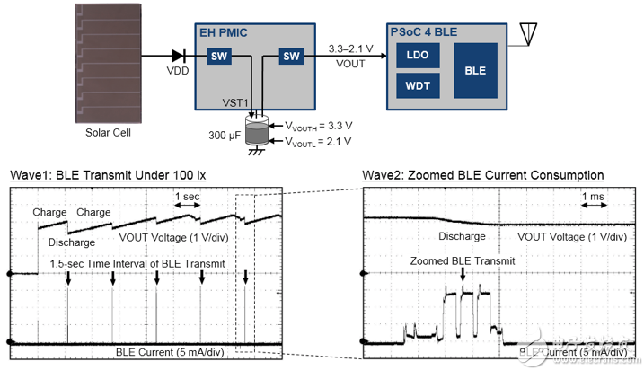
The block diagram in Figure 10 shows the energy harvesting process for PSoC 4 BLE based on the S6AE102A and S6AE103APSoC boards.
Wave1 shows a solar-based BLE run, and Wave2 shows the BLE current consumption at the time of transmission. The PMIC first stores the solar energy on a 300-μF ceramic capacitor on VSTORE1 (VST1). When VST1 reaches VVOUTH, energy is sent to the MCU for BLE operation.
[Figure 10 | Simple Energy Harvesting]
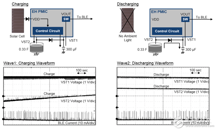
However, this simple energy harvesting process does not last for a full day without a backup capacitor (for example, during periods of no light).
The block diagram and waveforms in Figure 11 show the hybrid energy storage control function. The energy used to run the system is stored in VST1 and the remaining energy is used to charge VSTORE2 (VST2). When there is no ambient light, the VST2 can continue to provide energy to the system.
[Figure 11 | Mixed Energy Storage Control Function]
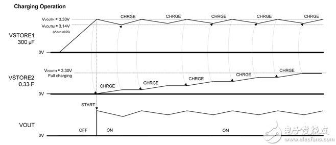
The waveform in Figure 12 shows the charging curve when energy is stored to VSTORE2. The S6AE10xA stores energy in VSTORE1 (small capacitor) and VSTORE2 (large capacitor). The energy stored in VSTORE1 is used for system operation and the remaining energy is used to charge the sub-storage device of VSTORE2 (VST2). VSTORE2 continues to power the system, so the system can continue to run for a while even in the absence of ambient light.
[Fig. 12 | Waveform for storing excess energy]
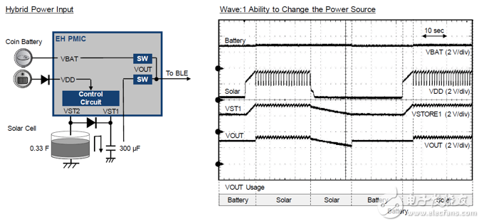
The block diagram in Figure 13 shows the hybrid power input control mode. Wave1 shows how the PMIC controls two power sources (solar and battery). The PMIC drives the system in different scenarios by converting these two power supplies. Ambient light is usually continuous, but there may be no continuous light in some places. The PMIC automatically converts the two power supplies and continues to supply power in the absence of light.
[Figure 13 | Hybrid Power Input Control]
The S6AE10xA automatically replaces the power supply based on the voltage of the VSTORE1. If the voltage of VSOTRE1 reaches VVOUTL, it will be powered from the VBAT supply to continue powering in the absence of ambient light.
Below are examples of how to implement different applications.
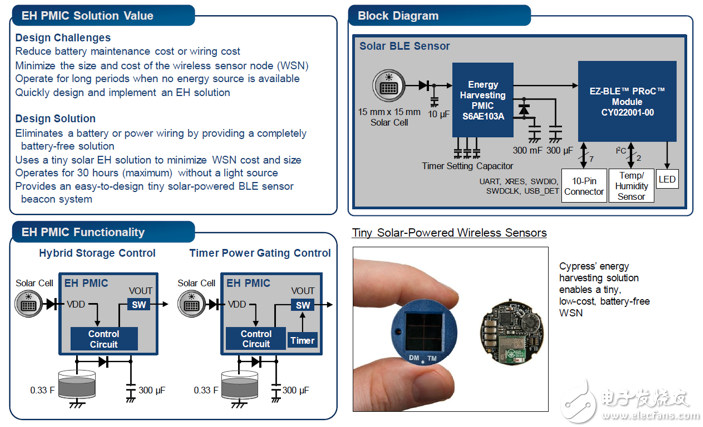
[Figure 14 | A compact solar wireless sensor that needs to run all day]
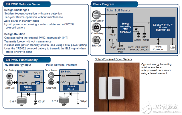
[Fig. 15 | Compact solar door sensor requiring short/frequent operation]
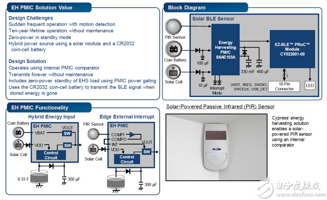
[Fig. 16 | Solar passive infrared sensor]
There are two types of noise canceling headphones, active noise reduction and passive noise reduction.
The active noise reduction function is to generate a reverse sound wave equal to the external noise through the noise reduction system, and neutralize the noise, thereby achieving the effect of noise reduction. Active noise canceling headphones with noise-reducing circuits that compete with external noise. Most of them use a large head-mounted design, which can be used to block external noise by using earplugs and earphone casings, and to perform the first round of sound insulation. There is plenty of room to install active noise reduction circuits and power supplies.
Passive noise canceling headphones mainly form an enclosed space by surrounding the ear, or use soundproof materials such as silicone earplugs to block external noise. Since the noise is not processed by the noise reduction circuit chip, generally only high frequency noise is blocked, and the noise reduction effect on the low frequency noise is not obvious.
Application:
1: Business people, because of frequent business trips, especially those who travel between different cities every day, they must hate the noise in the cabin. If there is a noise-cancelling earphone, they will be able to stay away from these noises. Relax by enjoying the music.
2: The office staff also need a pair of noise canceling headphones. Sometimes when thinking about planning, listening to the sound of central air conditioning is particularly annoying, and if there are colleagues around at this time, it is even more annoying. At this time, you may wear a pair of noise-cancelling headphones to expand your thinking in music.

Noise Cancelling Headphones,Wireless Noise Cancelling Headphones,Sound Cancelling Headphones,Bluetooth Noise Cancelling Headphones
Shenzhen Linx Technology Co., Ltd. , https://www.linxheadphone.com